SLVSCQ7 April 2015 TPS61046
PRODUCTION DATA.
- 1 Features
- 2 Applications
- 3 Description
- 4 Simplified Schematic
- 5 Revision History
- 6 Pin Configuration and Functions
- 7 Specifications
- 8 Detailed Description
- 9 Application and Implementation
- 10Power Supply Recommendations
- 11Layout
- 12Device and Documentation Support
- 13Mechanical, Packaging, and Orderable Information
8 Detailed Description
8.1 Overview
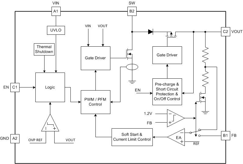
The TPS61046 is a highly integrated boost converter designed for applications requiring high voltage and tiny solution size such as PMOLED panel power supply and sensor module. The TPS61046 integrates a 30-V power switch, input/output isolation switch, and power diode. It can output up to 28 V from input of a Li+ battery or two cell alkaline batteries in series.
One common issue with conventional boost regulators is the conduction path from input to output even when the power switch is turned off. It creates three problems, which are inrush current during start-up, output leakage current during shutdown and excessive over load current. In the TPS61046, the isolation switch is turned off under shutdown mode and over load conditions, thereby opening the current path. Thus the TPS61046 can truely disconnect the load from the input voltage and minimize the leakage current during shutdown mode.
The TPS61046 operates with a switching frequency at 1.0 MHz. This allows the use of small external components. The TPS61046 has an internal default 12-V output voltage setting by connecting the FB pin to the VIN pin. Thus it only needs three external components to get 12-V output voltage. Together with WCSP package, the TPS61046 gives a very small overall solution size. The TPS61046 has typical 900-mA switch current limit. It has 10-ms built-in soft start time to minimize the inrush current. The TPS61064 also implements output short circuit protection, output over-voltage protection and thermal shutdown.
8.2 Functional Block Diagram

8.3 Feature Description
8.3.1 Under-Voltage Lockout
An under-voltage lockout (UVLO) circuit stops the operation of the converter when the input voltage drops below the typical UVLO threshold of 1.55 V. A hysteresis of 200 mV is added so that the device cannot be enabled again until the input voltage goes up to 1.75 V. This function is implemented in order to prevent malfunctioning of the device when the input voltage is between 1.55 V and 1.75 V.
8.3.2 Enable and Disable
When the input voltage is above maximal UVLO rising threshold of 1.8 V and the EN pin is pulled high, the TPS61046 is enabled. When the EN pin is pulled low, the TPS61046 goes into shutdown mode. The device stops switching and the isolation switch is turned off providing the isolation between input and output. In shutdown mode, less than 1-µA input current is consumed.
8.3.3 Soft Start
The TPS61046 begins soft start when the EN pin is pulled high. at the beginning of the soft start period, the isolation FET is turned on slowly to charge the output capacitor with 30-mA current for about 5 ms. This is called the pre-charge phase. After the pre-charge phase, the TPS61046 starts switching. This is called switching soft start phase. An internal soft start circuit limits the peak inductor current according to the output voltage. When the output voltage is below 3 V, the peak inductor current is limited to 140 mA. Along with the output voltage going up from 3 V to 5 V, the peak current limit is gradually increased to the normal value of 900 mA. The switching soft start phase is about 5 ms typically. The soft start funciton reduces the inrush current during startup.
8.3.4 Over-voltage Protection
The TPS61046 has internal output over-voltage protection (OVP) function. When the output voltage exceeds the OVP threshold of 29.2 V, the device stops switching. Once the output voltage falls 0.8 V below the OVP threshold, the device resumes operation again.
8.3.5 Output Short Circuit Protection
The TPS61046 starts to limit the output current whenever the output voltage drops below 4 V. The lower output voltage, the smaller output current limit. When the VOUT pin is shorted to ground, the output current is limited to less than 200 mA. This function protects the device from being damaged when the output is shorted to ground.
8.3.6 Thermal Shutdown
The TPS61046 goes into thermal shutdown once the junction temperature exceeds 150°C. When the junction temperature drops below the thermal shutdown temperature threshold less the hysteresis, typically 130°C, the device starts operating again.
8.3.7 Device Functional Modes
The TPS61046 has two operation modes, PWM mode and power save mode.
8.3.7.1 PWM Mode
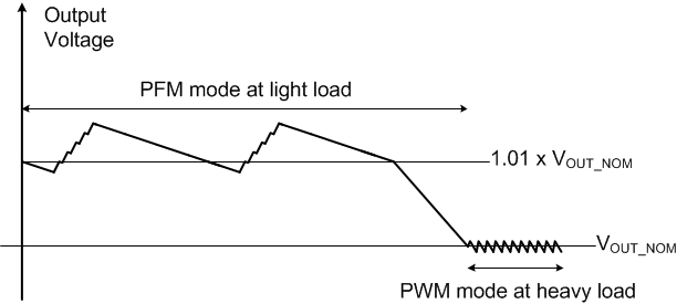
The TPS61046 uses a quasi-constant 1.0-MHz frequency pulse width modulation (PWM) at moderate to heavy load current. Based on the input voltage to output votlage ratio, a circuit predicts the required off-time. At the beginning of the switching cycle, the NMOS switching FET, shown in the functional block diagram, is turned on. The input voltage is applied across the inductor and the inductor current ramps up. In this phase, the output capacitor is discharged by the load current. When the inductor current hits the current threshold that is set by the output of the error amplifier, the PWM switch is turned off, and the power diode is forward-biased. The inductor transfers its stored energy to replenish the output capacitor and supply the load. When the off-time is expired, the next switching cycle starts again. The error amplifier compares the FB pin voltage with an internal reference votlage, and its output determines the inductor peak current.
The TPS61046 has a built-in compensation circuit that can accommodate a wide range of input voltage, output voltage, inductor value and output capacitor value for stable operation.
8.3.8 Power Save Mode
The TPS61046 integrates a power save mode with pulse frequency modulation (PFM) to improve efficiency at light load. When the load current decreases, the inductor peak current set by the output of the error amplifier declines to regulate the output voltage. When the inductor peak current hits the low limit of 140 mA, the output voltage will exceed the setting voltage as the load current decreases further. When the FB voltage hits the PFM reference voltage, the TPS61046 goes into the power save mode. In the power save mode, when the FB voltage rises and hits the PFM reference voltage, the device continuous switching for several cycles because of the delay time of the internal comparator. Then it stops switching. The load is supplied by the output capacitor and the output voltage declines. When the FB voltage falls below the PFM reference voltage, after the delay time of the comparator, the device starts switching again to ramp up the output voltage.
 Figure 10. Output Voltage in PWM Mode and PFM Mode