JAJSL03C January   2021  – December 2021 TPS61094

PRODUCTION DATA  

  1. 特長
  2. アプリケーション
  3. 概要
  4. Revision History
  5. Pin Configuration and Functions
  6. Specifications
    1. 6.1 Absolute Maximum Ratings
    2. 6.2 ESD Ratings
    3. 6.3 Recommended Operating Conditions
    4. 6.4 Thermal Information
    5. 6.5 Electrical Characteristics
    6. 6.6 Typical Characteristics
  7. Detailed Description
    1. 7.1 Overview
      1. 7.1.1 The Configuration of VCHG Pin, ICHG Pin, and OSEL Pin
        1. 7.1.1.1 OSEL: Output Voltage Selection
        2. 7.1.1.2 VCHG: Charging Termination Voltage Selection
        3. 7.1.1.3 ICHG: Charging Output Current Selection
    2. 7.2 Functional Block Diagram
    3. 7.3 Feature Description
      1. 7.3.1 Undervoltage Lockout
      2. 7.3.2 Enable and Soft Start
      3. 7.3.3 Active Pulldown for the EN and MODE Pins
      4. 7.3.4 Current Limit Operation
      5. 7.3.5 Output Short-to-Ground Protection
      6. 7.3.6 Thermal Shutdown
    4. 7.4 Device Functional Modes
      1. 7.4.1 Operation Mode Setting
      2. 7.4.2 Forced Bypass Mode Operation
      3. 7.4.3 True Shutdown Mode Operation
      4. 7.4.4 Forced Buck Mode Operation
      5. 7.4.5 Auto Buck or Boost Mode Operation
        1. 7.4.5.1 Three States (Boost_on, Buck_on, and Supplement) Transition
        2. 7.4.5.2 Boost, Bypass, and Pass-Through
        3. 7.4.5.3 PWM, PFM, and Snooze Modes in Boost Operation
          1. 7.4.5.3.1 PWM Mode
          2. 7.4.5.3.2 PFM Mode
          3. 7.4.5.3.3 Snooze Mode
  8. Application and Implementation
    1. 8.1 Application Information
    2. 8.2 Typical Application – 3.6-V Output Boost Converter with Bypass
      1. 8.2.1 Design Requirements
      2. 8.2.2 Detailed Design Procedure
        1. 8.2.2.1 Programming the Output Voltage
        2. 8.2.2.2 Maximum Output Current
        3. 8.2.2.3 Inductor Selection
        4. 8.2.2.4 Output Capacitor Selection
        5. 8.2.2.5 Input Capacitor Selection
      3. 8.2.3 Application Curves
      4. 8.2.4 Typical Application – 3.3-V Output Boost Converter with Automatic Buck or Boost Function
        1. 8.2.4.1 Design Requirements
        2. 8.2.4.2 Detailed Design Procedure
          1. 8.2.4.2.1 Programming the Voltage and Current
        3. 8.2.4.3 Application Curves
  9. Power Supply Recommendations
  10. 10Layout
    1. 10.1 Layout Guidelines
    2. 10.2 Layout Example
  11. 11Device and Documentation Support
    1. 11.1 Device Support
      1. 11.1.1 Third-Party Products Disclaimer
    2. 11.2 Documentation Support
      1. 11.2.1 Related Documentation
    3. 11.3 Receiving Notification of Documentation Updates
    4. 11.4 サポート・リソース
    5. 11.5 Trademarks
    6. 11.6 Electrostatic Discharge Caution
    7. 11.7 Glossary
  12. 12Mechanical, Packaging, and Orderable Information

パッケージ・オプション

メカニカル・データ(パッケージ|ピン)
サーマルパッド・メカニカル・データ
発注情報

Output Capacitor Selection

The output capacitor is mainly selected to meet the requirements for output ripple and loop stability. The ripple voltage is related to capacitor capacitance and its equivalent series resistance (ESR). Assuming a ceramic capacitor with zero ESR, the minimum capacitance needed for a given ripple voltage can be calculated by Equation 8.
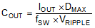
Equation 8. GUID-BBABEFA5-2D2F-48F7-89D0-472080409FFD-low.gif

where

  • DMAX is the maximum switching duty cycle.
  • VRIPPLE is the peak-to-peak output ripple voltage.
  • IOUT is the maximum output current.
  • fSW is the switching frequency.

The ESR impact on the output ripple must be considered if tantalum or aluminum electrolytic capacitors are used. The output peak-to-peak ripple voltage caused by the ESR of the output capacitors can be calculated by Equation 9.

Equation 9. GUID-1BA35956-154E-4063-AB64-B9CF0F28F405-low.gif

Take care when evaluating the derating of a ceramic capacitor under DC bias voltage, aging, and AC signal. For example, the DC bias voltage can significantly reduce capacitance. A ceramic capacitor can lose more than 50% of its capacitance at its rated voltage. Therefore, always leave margin on the voltage rating to make sure there is adequate capacitance at the required output voltage. Increasing the output capacitor makes the output ripple voltage smaller in PWM mode.

TI recommends using the X5R or X7R ceramic output capacitor in the range of 4-μF to 1000-μF effective capacitance. The output capacitor affects the small signal control loop stability of the boost regulator. If the output capacitor is below the range, the boost regulator can potentially become unstable. Increasing the output capacitor makes the output ripple voltage smaller in PWM mode.