JAJSL03C January   2021  – December 2021 TPS61094

PRODUCTION DATA  

  1. 特長
  2. アプリケーション
  3. 概要
  4. Revision History
  5. Pin Configuration and Functions
  6. Specifications
    1. 6.1 Absolute Maximum Ratings
    2. 6.2 ESD Ratings
    3. 6.3 Recommended Operating Conditions
    4. 6.4 Thermal Information
    5. 6.5 Electrical Characteristics
    6. 6.6 Typical Characteristics
  7. Detailed Description
    1. 7.1 Overview
      1. 7.1.1 The Configuration of VCHG Pin, ICHG Pin, and OSEL Pin
        1. 7.1.1.1 OSEL: Output Voltage Selection
        2. 7.1.1.2 VCHG: Charging Termination Voltage Selection
        3. 7.1.1.3 ICHG: Charging Output Current Selection
    2. 7.2 Functional Block Diagram
    3. 7.3 Feature Description
      1. 7.3.1 Undervoltage Lockout
      2. 7.3.2 Enable and Soft Start
      3. 7.3.3 Active Pulldown for the EN and MODE Pins
      4. 7.3.4 Current Limit Operation
      5. 7.3.5 Output Short-to-Ground Protection
      6. 7.3.6 Thermal Shutdown
    4. 7.4 Device Functional Modes
      1. 7.4.1 Operation Mode Setting
      2. 7.4.2 Forced Bypass Mode Operation
      3. 7.4.3 True Shutdown Mode Operation
      4. 7.4.4 Forced Buck Mode Operation
      5. 7.4.5 Auto Buck or Boost Mode Operation
        1. 7.4.5.1 Three States (Boost_on, Buck_on, and Supplement) Transition
        2. 7.4.5.2 Boost, Bypass, and Pass-Through
        3. 7.4.5.3 PWM, PFM, and Snooze Modes in Boost Operation
          1. 7.4.5.3.1 PWM Mode
          2. 7.4.5.3.2 PFM Mode
          3. 7.4.5.3.3 Snooze Mode
  8. Application and Implementation
    1. 8.1 Application Information
    2. 8.2 Typical Application – 3.6-V Output Boost Converter with Bypass
      1. 8.2.1 Design Requirements
      2. 8.2.2 Detailed Design Procedure
        1. 8.2.2.1 Programming the Output Voltage
        2. 8.2.2.2 Maximum Output Current
        3. 8.2.2.3 Inductor Selection
        4. 8.2.2.4 Output Capacitor Selection
        5. 8.2.2.5 Input Capacitor Selection
      3. 8.2.3 Application Curves
      4. 8.2.4 Typical Application – 3.3-V Output Boost Converter with Automatic Buck or Boost Function
        1. 8.2.4.1 Design Requirements
        2. 8.2.4.2 Detailed Design Procedure
          1. 8.2.4.2.1 Programming the Voltage and Current
        3. 8.2.4.3 Application Curves
  9. Power Supply Recommendations
  10. 10Layout
    1. 10.1 Layout Guidelines
    2. 10.2 Layout Example
  11. 11Device and Documentation Support
    1. 11.1 Device Support
      1. 11.1.1 Third-Party Products Disclaimer
    2. 11.2 Documentation Support
      1. 11.2.1 Related Documentation
    3. 11.3 Receiving Notification of Documentation Updates
    4. 11.4 サポート・リソース
    5. 11.5 Trademarks
    6. 11.6 Electrostatic Discharge Caution
    7. 11.7 Glossary
  12. 12Mechanical, Packaging, and Orderable Information

パッケージ・オプション

メカニカル・データ(パッケージ|ピン)
サーマルパッド・メカニカル・データ
発注情報

Pin Configuration and Functions

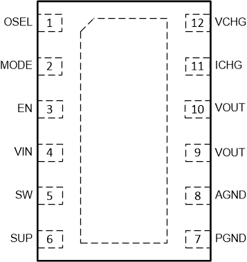
GUID-53BA5808-D8B1-4662-9EAC-842FEA34D352-low.gif Figure 5-1 12-Pin WSONDSS Package(Top View)
Table 5-1 Pin Functions
PIN I/O(1) DESCRIPTION
NO. NAME
1 OSEL I Boost output voltage selection pin. Connect a resistor between this pin and ground to select one of sixteen output voltages of Boost mode.
2 MODE I Operation mode selection pin. The MODE pin and EN pin work together to set device operation mode. See Table 7-4.
3 EN I Operation mode selection pin. The MODE pin and EN pin work together to set device operation mode. See Table 7-4.
4 VIN PWR IC power supply input
5 SW PWR The switching node pin of the converter. It is connected to the drain of the internal low-side power MOSFET and the source of the internal high-side power MOSFET.
6 SUP I Output of buck converter to sense the voltage of the supercap
7 PGND PWR Power ground
8 AGND PWR Signal ground
9, 10 VOUT PWR Output of the device
11 ICHG I Charging current selection pin. Connect a resistor between this pin and ground to select one of sixteen output currents of Buck mode.
12 VCHG I Charging voltage selection pin. Connect a resistor between this pin and ground to select one of sixteen regulation voltages of Buck mode.
I = Input, PWR = Power