JAJSL03C January   2021  – December 2021 TPS61094

PRODUCTION DATA  

  1. 特長
  2. アプリケーション
  3. 概要
  4. Revision History
  5. Pin Configuration and Functions
  6. Specifications
    1. 6.1 Absolute Maximum Ratings
    2. 6.2 ESD Ratings
    3. 6.3 Recommended Operating Conditions
    4. 6.4 Thermal Information
    5. 6.5 Electrical Characteristics
    6. 6.6 Typical Characteristics
  7. Detailed Description
    1. 7.1 Overview
      1. 7.1.1 The Configuration of VCHG Pin, ICHG Pin, and OSEL Pin
        1. 7.1.1.1 OSEL: Output Voltage Selection
        2. 7.1.1.2 VCHG: Charging Termination Voltage Selection
        3. 7.1.1.3 ICHG: Charging Output Current Selection
    2. 7.2 Functional Block Diagram
    3. 7.3 Feature Description
      1. 7.3.1 Undervoltage Lockout
      2. 7.3.2 Enable and Soft Start
      3. 7.3.3 Active Pulldown for the EN and MODE Pins
      4. 7.3.4 Current Limit Operation
      5. 7.3.5 Output Short-to-Ground Protection
      6. 7.3.6 Thermal Shutdown
    4. 7.4 Device Functional Modes
      1. 7.4.1 Operation Mode Setting
      2. 7.4.2 Forced Bypass Mode Operation
      3. 7.4.3 True Shutdown Mode Operation
      4. 7.4.4 Forced Buck Mode Operation
      5. 7.4.5 Auto Buck or Boost Mode Operation
        1. 7.4.5.1 Three States (Boost_on, Buck_on, and Supplement) Transition
        2. 7.4.5.2 Boost, Bypass, and Pass-Through
        3. 7.4.5.3 PWM, PFM, and Snooze Modes in Boost Operation
          1. 7.4.5.3.1 PWM Mode
          2. 7.4.5.3.2 PFM Mode
          3. 7.4.5.3.3 Snooze Mode
  8. Application and Implementation
    1. 8.1 Application Information
    2. 8.2 Typical Application – 3.6-V Output Boost Converter with Bypass
      1. 8.2.1 Design Requirements
      2. 8.2.2 Detailed Design Procedure
        1. 8.2.2.1 Programming the Output Voltage
        2. 8.2.2.2 Maximum Output Current
        3. 8.2.2.3 Inductor Selection
        4. 8.2.2.4 Output Capacitor Selection
        5. 8.2.2.5 Input Capacitor Selection
      3. 8.2.3 Application Curves
      4. 8.2.4 Typical Application – 3.3-V Output Boost Converter with Automatic Buck or Boost Function
        1. 8.2.4.1 Design Requirements
        2. 8.2.4.2 Detailed Design Procedure
          1. 8.2.4.2.1 Programming the Voltage and Current
        3. 8.2.4.3 Application Curves
  9. Power Supply Recommendations
  10. 10Layout
    1. 10.1 Layout Guidelines
    2. 10.2 Layout Example
  11. 11Device and Documentation Support
    1. 11.1 Device Support
      1. 11.1.1 Third-Party Products Disclaimer
    2. 11.2 Documentation Support
      1. 11.2.1 Related Documentation
    3. 11.3 Receiving Notification of Documentation Updates
    4. 11.4 サポート・リソース
    5. 11.5 Trademarks
    6. 11.6 Electrostatic Discharge Caution
    7. 11.7 Glossary
  12. 12Mechanical, Packaging, and Orderable Information

パッケージ・オプション

メカニカル・データ(パッケージ|ピン)
サーマルパッド・メカニカル・データ
発注情報

Inductor Selection

Because the selection of the inductor affects steady-state operation, transient behavior, and loop stability, the inductor is the most important component in power regulator design. There are three important inductor specifications: inductor value, saturation current, and DC resistance (DCR).

The TPS61094 is designed to work with 1-µH or 2.2-µH inductor values. Follow Equation 5 to Equation 7 to calculate the inductor peak current for the application. To calculate the current in the worst case, use the minimum input voltage, maximum output voltage, and maximum load current of the application. To have enough design margins, choose the inductor value with –30% tolerances and low power-conversion efficiency for the calculation.

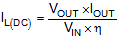
In a boost regulator, the inductor DC current can be calculated by Equation 5.

Equation 5. GUID-6B157077-5D97-4E84-ABCB-8E5B66E086AE-low.gif

where

  • VOUT is the output voltage of the boost converter.
  • IOUT is the output current of the boost converter.
  • VIN is the input voltage of the boost converter.
  • η is the power conversion efficiency, use 90% for most applications.

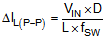
The inductor ripple current is calculated by Equation 6.

Equation 6. GUID-24F23D2C-C25D-4010-8B39-4EBF4FAA9231-low.gif

where

  • D is the duty cycle, which can be calculated by Equation 2.
  • L is the inductance value of the inductor.
  • fSW is the switching frequency.
  • VIN is the input voltage of the boost converter.

Therefore, the inductor peak current is calculated by Equation 7.

Equation 7. GUID-D5D27918-A169-4E97-A928-C5B3AC8C8B44-low.gif

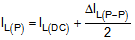
Normally, it is advisable to work with an inductor peak-to-peak current of less than 40% of the average inductor current for maximum output current. A smaller ripple from a larger-valued inductor reduces the magnetic hysteresis losses in the inductor and EMI, but in the same way, load transient response time is increased. The saturation current of the inductor must be higher than the calculated peak inductor current. Table 8-2 lists the recommended inductors for the TPS61094.

Table 8-2 Recommended Inductors for the TPS61094
PART NUMBER L (µH) DCR MAX (mΩ) SATURATION CURRENT (A) SIZE (LxWxH) VENDOR(1)
XGL4020-222ME 2.2 21.5 4.4 4.0 × 4.0 × 2.1 Coilcraft
VCHA042A-2R2MS6 2.2 23.0 4.5 4.3 x 4.3 x 2.1 Cyntec
744383560 22 2.2 35.0 6.2 4.1 x 4.1 x 2.1 Wurth Elecktronik
See the Third-Party Products disclaimer