SLVS789D November 2007 – December 2014 TPS61170
PRODUCTION DATA.
- 1 Features
- 2 Applications
- 3 Description
- 4 Typical Application Schematic
- 5 Revision History
- 6 Pin Configuration and Functions
- 7 Specifications
- 8 Detailed Description
- 9 Application and Implementation
- 10Power Supply Recommendations
- 11Layout
- 12Device and Documentation Support
- 13Mechanical, Packaging, and Orderable Information
9 Application and Implementation
NOTE
Information in the following applications sections is not part of the TI component specification, and TI does not warrant its accuracy or completeness. TI’s customers are responsible for determining suitability of components for their purposes. Customers should validate and test their design implementation to confirm system functionality.
9.1 Application Information
The TPS6170 is designed for output voltages up to 38 V with a switch peak current limit of 0.96-A minimum. The device, which operates in peak current mode PWM control, is externally compensated for maximum flexibility and stability. The switching frequency is fixed at 1.2 MHz, and the input voltage range is 3.0 to 18 V. The following section provides a step-by-step design approach for configuring the TPS61170 as a voltage regulating boost converter.
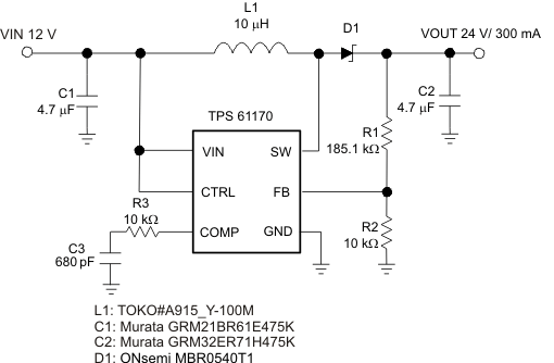
9.2 Typical Application
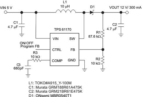 Figure 12. 5-V to 12-V DCDC Power Conversion With Programmable Feedback Reference Voltage
9.2.1 Design Requirements
Table 4. TPS61170 12-V Output Design Requirements
| PARAMETERS | VALUES |
|---|---|
| Input Voltage | 5.0V ± 20% |
| Output Voltage | 12V |
| Output Current | 300mA |
9.2.2 Detailed Design Procedure
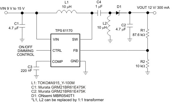
9.2.2.1 Program Output Voltage
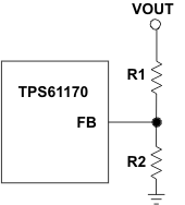 Figure 13. Program Output Voltage
To program the output voltage, select the values of R1 and R2 (see Figure 13) according to Equation 2.
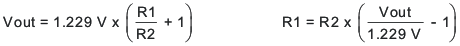
Considering the leakage current through the resistor divider and noise decoupling to FB pin, an optimum value for R2 is around 10k. The output voltage tolerance depends on the accuracy of the reference voltage and the tolerance of R1 and R2.
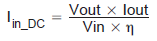
9.2.2.2 Maximum Output Current
The overcurrent limit in a boost converter limits the maximum input current, and thus the maximum input power for a given input voltage. The maximum output power is less than the maximum input power due to power conversion losses. Therefore, the current-limit setting, input voltage, output voltage and efficiency can all affect the maximum output current. The current limit clamps the peak inductor current; therefore, the ripple must be subtracted to derive the maximum DC current. The ripple current is a function of the switching frequency, inductor value and duty cycle. The following equations take into account of all the above factors for maximum output current calculation.
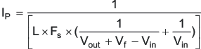
where:
IP = inductor peak to peak ripple current
L = inductor value
Vf = Schottky diode forward voltage
Fs = switching frequency
Vout = output voltage
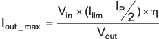
where:
Iout_max = Maximum output current of the boost converter
Ilim = overcurrent limit
η = efficiency
For instance, when Vin is 5 V, Vout is 12 V, the inductor is 10 μH, the Schottky forward voltage is 0.2 V; and then the maximum output current is 300 mA in a typical operation.
9.2.2.3 Switch Duty Cycle
The maximum switch duty cycle (D) of the TPS61170 is 90% (min). The duty cycle of a boost converter under continuous conduction mode (CCM) is given by:
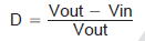
For a 5 V to 12 V application, the duty cycle is 58.3%, and for a 5 V to 24 V application, the duty cycle is 79.2%. The duty cycle must be lower than the maximum specification of 90% in the application; otherwise, the output voltage cannot be regulated.
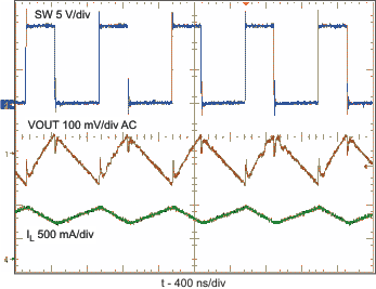
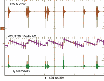
Once the PWM switch is turned on, the TPS61170 has minimum ON pulse width. This sets the limit of the minimum duty cycle. When operating at low duty cycles, the TPS61170 enters pulse-skipping mode. In this mode, the device turns the power switch off for several switching cycles to prevent the output voltage from rising above regulation. This operation typically occurs in light load condition when the PWM operates in discontinuous mode. See the Figure 17.
9.2.2.4 Inductor Selection
The selection of the inductor affects steady state operation as well as transient behavior and loop stability. These factors make it the most important component in power regulator design. There are three important inductor specifications: inductor value, DC resistance (DCR) and saturation current. Considering inductor value alone is not enough.
The inductance value of the inductor determines its ripple current. It is recommended that the peak-to-peak ripple current given by Equation 3 be set to 30–40% of the DC current. Inductance values shown in Recommended Operating Conditions are recommended for most applications. Inductor DC current can be calculated as
Inductor values can have ±20% tolerance with no current bias. When the inductor current approaches saturation level, its inductance can decrease 20% to 35% from the 0A value depending on how the inductor vendor defines saturation current. Using an inductor with a smaller inductance value forces discontinuous PWM where the inductor current ramps down to zero before the end of each switching cycle. This reduces the boost converter’s maximum output current, causes large input voltage ripple and reduces efficiency. In general, inductors with large inductance and low DCR values provide much more output current and higher conversion efficiency. Inductors with smaller inductance values can give better load transient response. For these reasons, a 10 μH to 22 μH inductance value range is recommended. Table 5 lists some recommended inductors for the TPS61170.
TPS61170 has built-in slope compensation to avoid subharmonic oscillation associated with current mode control. If the inductor value is lower than 10 μH, the slope compensation may not be adequate, and the loop can become unstable. Therefore, customers need to verify operation in their application if the inductor is different from the recommended values.
Table 5. Recommended Inductors for TPS61170
| PART NUMBER | L (μH) |
DCR MAX (mΩ) |
SATURATION CURRENT (A) |
SIZE (L × W × H mm) |
VENDOR |
|---|---|---|---|---|---|
| A915_Y-100M | 10 | 90 | 1.3 | 5.2 × 5.2 × 3.0 | TOKO |
| VLCF5020T-100M1R1-1 | 10 | 237 | 1.1 | 5 × 5×2.0 | TDK |
| CDRH4D22/HP | 10 | 144 | 1.2 | 5 × 5 × 2.4 | Sumida |
| LQH43PN100MR0 | 10 | 247 | 0.84 | 4.5 × 3.2 × 2.0 | Murata |
9.2.2.5 Schottky Diode Selection
The high switching frequency of the TPS61170 demands a high-speed rectifying switch for optimum efficiency. Ensure that the average and peak current rating of the diode exceeds the average output current and peak inductor current. In addition, the reverse breakdown voltage of the diode must exceed the switch FET rating voltage of 40 V. So, the ONSemi MBR0540 is recommended for TPS61170. However, Schottky diodes with lower rated voltages can be used for lower output voltages to save the solution size and cost. For example, a converter providing a 12-V output with 20-V diode is a good choice.
9.2.2.6 Compensation Capacitor Selection
The TPS61170 has an external compensation, COMP pin, which allows the loop response to be optimized for each application. The COMP pin is the output of the internal error amplifier. An external resistor R3 and ceramic capacitor C3 are connected to COMP pin to provide a pole and a zero. This pole and zero, along with the inherent pole of a current mode control boost converter, determine the close loop frequency response. This is important to a converter stability and transient response.
The following equations summarize the poles, zeros and DC gain of a TPS61170 boost converter with ceramic output capacitor (C2), as shown in the block diagram. They include the dominant pole (fP1), the output pole (fP2) of a boost converter, the right-half-plane zero (fRHPZ) of a boost converter, the zero (fZ) generated by R3 and C3, and the DC gain (A).
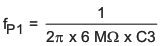
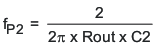
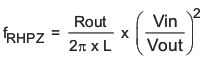
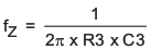
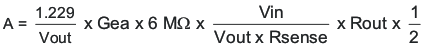
where Rout is the load resistance, Gea is the error amplifier transconductance located in Electrical Characteristics, Rsense (100mΩ typical) is a sense resistor in the current control loop. These equations helps generate a simple bode plot for TPS61170 loop analysis.
Increasing R3 or reducing C3 increases the close loop bandwidth which improves the transient response. Adjusting R3 and C3 in opposite directions increase the phase, and help loop stability. For many of the applications, the recommended value of 10k and 680pF makes an ideal compromise between transient response and loop stability. To optimize the compensation, use C3 in the range of 100pF to 10nF, and R3 of 10k. See the TI application report SLVA319 for thorough analysis and description of the boost converter small signal model and compensation design.
9.2.2.7 Input and Output Capacitor Selection
The output capacitor is mainly selected to meet the requirements for the output ripple and loop stability. The ripple voltage is related to the capacitor’s capacitance and its equivalent series resistance (ESR). Assuming a capacitor with zero ESR, the minimum capacitance needed for a given ripple can be calculated using Equation 12.
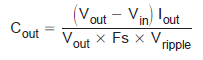
Where, Vripple = peak-to-peak output ripple. The additional output ripple component caused by ESR is calculated using:
Due to its low ESR, Vripple_ESR can be neglected for ceramic capacitors, but must be considered if tantalum or electrolytic capacitors are used.
Care must be taken when evaluating a ceramic capacitor’s derating under dc bias, aging and AC signal. For example, larger form factor capacitors (in 1206 size) have a resonant frequencies in the range of the switching frequency. So, the effective capacitance is significantly lower. The DC bias can also significantly reduce capacitance. Ceramic capacitors can lose as much as 50% of its capacitance at its rated voltage. Therefore, choose a ceramic capacitor with a voltage rating at least 1.5X its expected dc bias voltage.
The capacitor in the range of 1 μF to 4.7 μF is recommended for input side. The output typically requires a capacitor in the range of 1 μF to 10 μF. The output capacitor affects the loop stability of the boost regulator. If the output capacitor is below the range, the boost regulator can potentially become unstable.
The popular vendors for high value ceramic capacitors are:
TDK (http://www.component.tdk.com/components.php)
Murata (http://www.murata.com/cap/index.html)
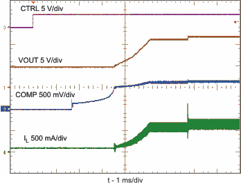
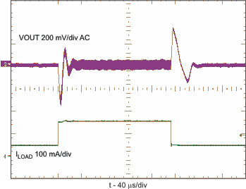
9.2.3 Application Curves