SLVS776B January   2009  – November 2014 TPS61220 , TPS61221 , TPS61222

PRODUCTION DATA.  

  1. Features
  2. Applications
  3. Description
  4. Simplified Schematic
  5. Revision History
  6. Pin Configuration and Functions
  7. Specifications
    1. 7.1 Absolute Maximum Ratings
    2. 7.2 Handling Ratings
    3. 7.3 Recommended Operating Conditions
    4. 7.4 Thermal Information
    5. 7.5 Electrical Characteristics
    6. 7.6 Typical Characteristics
  8. Parameter Measurement Information
  9. Detailed Description
    1. 9.1 Overview
    2. 9.2 Functional Block Diagrams
    3. 9.3 Feature Description
      1. 9.3.1 Controller Circuit
      2. 9.3.2 Device Enable And Shutdown Mode
      3. 9.3.3 Startup
      4. 9.3.4 Operation At Output Overload
      5. 9.3.5 Undervoltage Lockout
      6. 9.3.6 Overvoltage Protection
      7. 9.3.7 Overtemperature Protection
    4. 9.4 Device Functional Modes
  10. 10Applications and Implementation
    1. 10.1 Application Information
    2. 10.2 Typical Applications
      1. 10.2.1 Specific Application, Fixed Output Voltage Supply
        1. 10.2.1.1 Design Requirements
        2. 10.2.1.2 Detailed Design Procedure
          1. 10.2.1.2.1 Device Choice
          2. 10.2.1.2.2 Programming The Output Voltage
          3. 10.2.1.2.3 Inductor Selection
          4. 10.2.1.2.4 Capacitor Selection
            1. 10.2.1.2.4.1 Input Capacitor
            2. 10.2.1.2.4.2 Output Capacitor
        3. 10.2.1.3 Application Curves
      2. 10.2.2 Specific Application, Variable Output Voltage Supply
        1. 10.2.2.1 Design Requirements
        2. 10.2.2.2 Detailed Design Procedure
          1. 10.2.2.2.1 Device Selection
          2. 10.2.2.2.2 Programming The Output Voltage
          3. 10.2.2.2.3 Inductor Selection
          4. 10.2.2.2.4 Capacitor Selection
        3. 10.2.2.3 Application Curves
  11. 11Power Supply Recommendations
    1. 11.1 Typical Power Sources
    2. 11.2 Input Voltage Effects On Output Current and Efficiency
    3. 11.3 Behavior While Disabled
    4. 11.4 Startup
  12. 12Layout
    1. 12.1 Layout Guidelines
    2. 12.2 Layout Example
    3. 12.3 Thermal Considerations
  13. 13Device and Documentation Support
    1. 13.1 Device Support
      1. 13.1.1 Third-Party Products Disclaimer
      2. 13.1.2 Development Support
    2. 13.2 Documentation Support
      1. 13.2.1 Related Documentation
    3. 13.3 Related Links
    4. 13.4 Trademarks
    5. 13.5 Electrostatic Discharge Caution
    6. 13.6 Glossary
  14. 14Mechanical, Packaging, and Orderable Information
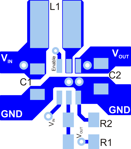
パッケージ・オプション

メカニカル・データ(パッケージ|ピン)
サーマルパッド・メカニカル・データ

12 Layout

12.1 Layout Guidelines

As for all switching power supplies, the layout is an important step in the design, especially at high peak currents and high switching frequencies. If the layout is not carefully done, the regulator could show stability problems as well as EMI problems. Therefore, use wide and short traces for the main current path and for the power ground paths. The input and output capacitor, as well as the inductor should be placed as close as possible to the IC.

The feedback divider in an application using the TPS61220 should be placed as close as possible to the control ground pin of the IC. To route the ground path from the resistor divider, use short traces as well, separated from the power ground traces. This avoids ground shift problems, which can occur due to superimposition of power ground current and control ground current. Assure that the ground traces are connected close to the device GND pin.

12.2 Layout Example

layout2_slvs776.gifFigure 30. PCB Layout Suggestion For Adjustable Output Voltage Options

12.3 Thermal Considerations

Implementation of integrated circuits in low-profile and fine-pitch surface-mount packages typically requires special attention to power dissipation. Many system-dependent issues such as thermal coupling, airflow, added heat sinks and convection surfaces, and the presence of other heat-generating components affect the power-dissipation limits of a given component.

Three basic approaches for enhancing thermal performance are listed below.

  • Improving the power-dissipation capability of the PCB design
  • Improving the thermal coupling of the component to the PCB
  • Introducing airflow in the system

For more details on how to use the thermal parameters in the dissipation ratings table please check the Thermal Characteristics Application Note (SZZA017) and the IC Package Thermal Metrics Application Note (SPRA953).