SLVSAO4C December 2010 – June 2020 TPS61240-Q1
PRODUCTION DATA.
- 1 Features
- 2 Applications
- 3 Description
- 4 Revision History
- 5 Pin Configuration and Functions
- 6 Specifications
- 7 Detailed Description
- 8 Application and Implementation
- 9 Power Supply Recommendations
- 10Layout
- 11Device and Documentation Support
- 12Mechanical, Packaging, and Orderable Information
パッケージ・オプション
メカニカル・データ(パッケージ|ピン)
- DRV|6
サーマルパッド・メカニカル・データ
- DRV|6
発注情報
3 Description
The TPS61240-Q1 device is a high efficient synchronous step up DC-DC converter optimized for products powered by either a three-cell alkaline, NiCd or NiMH, or one-cell Li-Ion or Li-Polymer battery. The TPS61240-Q1 supports output currents up to 450 mA. The TPS61240-Q1 has an input valley current limit of 500 mA.
TPS61240-Q1 device provides fixed output voltage of 5V-typ with an input voltage range of 2.3 V to 5.5 V and the device supports batteries with extended voltage range. During shutdown, the load is completely disconnected from the battery. The TPS61240-Q1 boost converter is based on a quasi-constant on-time valley current mode control scheme.
The TPS61240-Q1 presents a high impedance at the VOUT pin when shut down. This allows for use in applications that require the regulated output bus to be driven by another supply while the TPS61240-Q1 is shut down.
During light loads the device will automatically pulse skip allowing maximum efficiency at lowest quiescent currents. In the shutdown mode, the current consumption is reduced to less than 1 μA.
TPS61240-Q1 allows the use of a small inductor and capacitors to achieve a small solution size. The TPS61240-Q1 is available in a 2 mm × 2 mm WSON package.
Device Information(1)
| PART NUMBER | PACKAGE | BODY SIZE (NOM) |
|---|---|---|
| TPS61240-Q1 | WSON (6) | 2.00 mm × 2.00 mm |
- For all available packages, see the orderable addendum at the end of the data sheet.
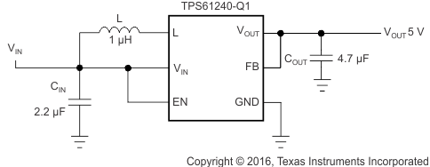
Simplified Schematic
