SLVSBX9A September 2014 – September 2014 TPS61291
PRODUCTION DATA.
- 1 Features
- 2 Applications
- 3 Description
- 4 Revision History
- 5 Pin Configuration and Functions
- 6 Specifications
- 7 Detailed Description
- 8 Applications and Implementation
- 9 Power Supply Recommendations
- 10Layout
- 11Device and Documentation Support
- 12Mechanical, Packaging, and Orderable Information
パッケージ・オプション
メカニカル・データ(パッケージ|ピン)
- DRV|6
サーマルパッド・メカニカル・データ
- DRV|6
発注情報
10 Layout
10.1 Layout Guidelines
As for all switching power supplies, the layout is an important step in the design. Care must be taken in board layout to get the specified performance. If the layout is not carefully done, the regulator could show poor line and/or load regulation, stability issues as well as EMI problems. It is critical to provide a low inductance, low impedance ground path. Therefore, use wide and short traces for the main current paths. In a boost converter, the ripple current on the output is larger than the ripple current on the input. The output capacitor needs to be placed as close as possible between the VOUT and the GND pins. The input capacitor should be placed as close as possible to the VIN and GND pins. Place the inductor close by the IC and connect it with short and thick traces to the IC. Avoid current loops to minimize radiated noise and stray fields. The exposed thermal pad of the package and the GND pin must be connected. See Figure 28 for the recommended PCB layout.
10.2 Layout Example
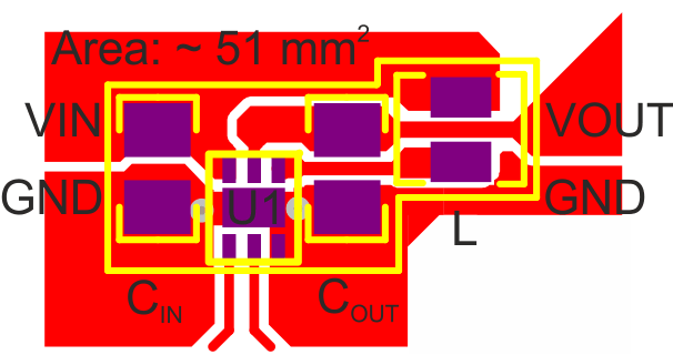 Figure 28. Recommended PCB Layout