SLVSBX9A September 2014 – September 2014 TPS61291
PRODUCTION DATA.
- 1 Features
- 2 Applications
- 3 Description
- 4 Revision History
- 5 Pin Configuration and Functions
- 6 Specifications
- 7 Detailed Description
- 8 Applications and Implementation
- 9 Power Supply Recommendations
- 10Layout
- 11Device and Documentation Support
- 12Mechanical, Packaging, and Orderable Information
パッケージ・オプション
メカニカル・データ(パッケージ|ピン)
- DRV|6
サーマルパッド・メカニカル・データ
- DRV|6
発注情報
6 Specifications
6.1 Absolute Maximum Ratings
over operating free-air temperature range (unless otherwise noted) (1)| MIN | MAX | UNIT | ||
|---|---|---|---|---|
| Pin Voltage Range (2) | VIN | -0.3 | 5.5 | V |
| SW | -0.3 | 7 | ||
| EN/BYP, VOUT | -0.3 | 5.5 | ||
| VSEL | -0.3 | VOUT + 0.3V | ||
| Output Current | In Bypass Operation (EN/BYP = GND) | 250 | mA | |
| TJ | Maximum Junction Temperature | -40 | 150 | °C |
(1) Stresses beyond those listed under Absolute Maximum Ratings may cause permanent damage to the device. These are stress ratings only, which do not imply functional operation of the device at these or any other conditions beyond those indicated under Recommended Operating Conditions. Exposure to absolute-maximum-rated conditions for extended periods may affect device reliability.
(2) All voltage values are with respect to network ground terminal GND.
6.2 Handling Ratings
| MIN | MAX | UNIT | |||
|---|---|---|---|---|---|
| Tstg | Storage temperature range | –65 | 150 | °C | |
| V(ESD) | Electrostatic discharge | Human body model (HBM) per ANSI/ESDA/JEDEC JS-001, all pins(1) | -2 | 2 | kV |
| Charged device model (CDM), per JEDEC specification JESD22-C101, all pins(2) | -0.5 | 0.5 | |||
(1) JEDEC document JEP155 states that 500-V HBM allows safe manufacturing with a standard ESD control process.
(2) JEDEC document JEP157 states that 250-V CDM allows safe manufacturing with a standard ESD control process.
6.3 Recommended Operating Conditions
over operating free-air temperature range (unless otherwise noted)| MIN | NOM | MAX | UNIT | ||
|---|---|---|---|---|---|
| VIN | Supply voltage for startup | 1.5 | V | ||
| Supply voltage range (once device has started) | 0.9 | 5 | |||
| Supply voltage range for step up conversion (once device has started) | 0.9 | VOUT | |||
| TA | Operating ambient temperature | -40 | 85 | °C | |
| TJ | Operating junction temperature | –40 | 125 | ||
6.4 Thermal Information
| THERMAL METRIC(1) | TPS61291 | UNIT | |
|---|---|---|---|
| DRV (2x2 SON) | |||
| 6 PINS | |||
| RθJA | Junction-to-ambient thermal resistance | 71.2 | °C/W |
| RθJCtop | Junction-to-case (top) thermal resistance | 93.5 | |
| RθJB | Junction-to-board thermal resistance | 46.7 | |
| ψJT | Junction-to-top characterization parameter | 2.5 | |
| ψJB | Junction-to-board characterization parameter | 41.1 | |
| RθJCbot | Junction-to-case (bottom) thermal resistance | 11.1 | |
(1) For more information about traditional and new thermal metrics, see the IC Package Thermal Metrics application report, SPRA953.
6.5 Electrical Characteristics
TA = –40°C to 85°C. Typical values are at TA = 25°C (unless otherwise noted)| PARAMETER | TEST CONDITIONS | MIN | TYP | MAX | UNIT | ||
|---|---|---|---|---|---|---|---|
| SUPPLY | |||||||
| VIN | Startup voltage | VOUT = 3.3V, IOUT = 20mA | 1.5 | V | |||
| Input voltage range | Operating voltage range | 0.9 | 5 | ||||
| IQ | Quiescent current in boost mode | VIN | IOUT = 0 mA, VEN/BYP = VIN = 1.8 V, VOUT = 3.3V, device not switching | 0.4 | 1.5 | μA | |
| VOUT | 5.7 | 9 | |||||
| Quiescent current in bypass mode | VIN | VEN/BYP = low, VIN = 3 V, IOUT = 0 mA | 0.015 | 0.5 | |||
| ILkSW | Leakage current into SW | VEN/BYP = low, VIN = 1.2 V, VSW = 1.2 V | 0.01 | 0.5 | μA | ||
| VUVLO | Undervoltage lockout threshold | VIN decreasing | 0.65 | 0.9 | V | ||
| Overtemperature protection | TJ rising | 140 | °C | ||||
| Overtemperature hysteresis | 20 | °C | |||||
| INPUTS | |||||||
| IIN | EN/BYP, input current | EN/BYP = low or EN/BYP = VIN | 0.01 | 0.1 | μA | ||
| VIL | EN/BYP, input low voltage | VIN ≤ 1.5 V | 0.2 × VIN | V | |||
| 5 V > VIN > 1.5 V | 0.3 | ||||||
| VIH | EN/BYP, input high voltage | VIN ≤ 1.5 V | 0.8 × VIN | V | |||
| 5 V > VIN > 1.5 V | 1.2 | ||||||
| VIL | VSEL, input low voltage | VEN/BYP = high | 0.3 | V | |||
| VIH | VSEL, input high voltage | VEN/BYP = high | VOUT - 0.3 | V | |||
| IIN | VSEL, input current | VEN/BYP = high, VSEL = VOUT = 3V | 0.01 | 0.1 | μA | ||
| POWER SWITCHES | |||||||
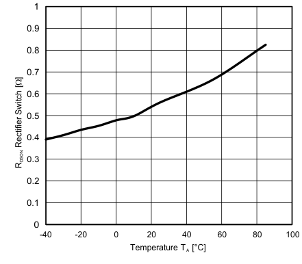
| RDS(ON) | Rectifying switch on resistance | VOUT = 3.3 V | 0.6 | Ω | |||
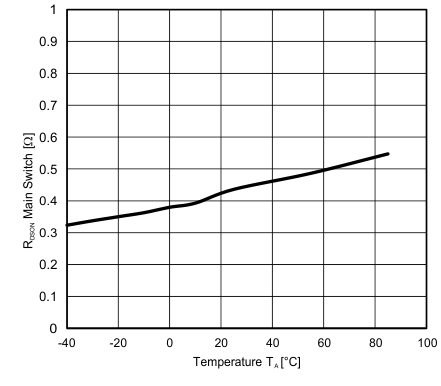
| Main switch on resistance | VOUT = 3.3 V | 0.4 | Ω | ||||
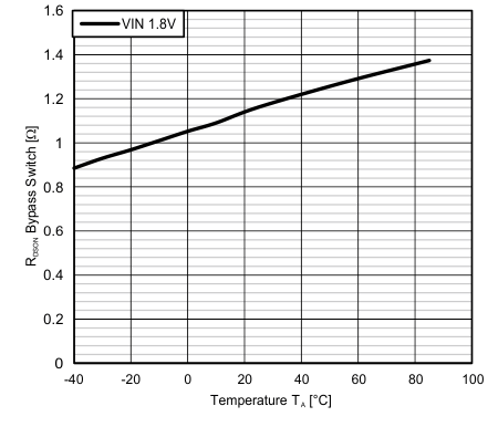
| Bypass switch on resistance | VIN = 1.8V, IOUT = 50 mA, EN/BYP = low | 1.2 | Ω | ||||
| ISW | Switch current limit | VOUT = 3.3V | 700 | 1000 | 1300 | mA | |
| OUTPUT | |||||||
| VOUT | Output voltage accuracy | VIN = 1.8V, IOUT = 10 mA, VOUT 3.3V, 3.0V, 2.5V, EN/BYP = high | -2 | +1 | +4 | % | |
| Line regulation | VOUT = 3.3V, VIN = 2V to 3.0V, IOUT = 50 mA, EN/BYP = high | +0.15 | %/V | ||||
| Load regulation | VIN = 2V, VOUT = 3.3V, IOUT = 1 mA to 200 mA, EN/BYP = high | -0.007 | %/mA | ||||
| VOVP | Output overvoltage protection | VOUT rising, EN/BYP = high | 5.4 | V | |||
6.6 Typical Characteristics
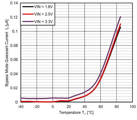
| EN/BYP = low | VSEL = low | IOUT = 0mA |
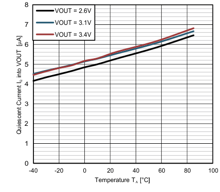
| EN/BYP = high | Boost mode operation | |
| IOUT = 0mA | Device not switching | |
| VOUT = 3.3V |
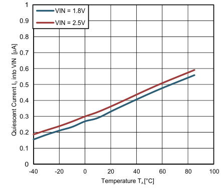
| EN/BYP = high | Boost mode operation | |
| Device not switching | ||
| VOUT = 3.3V |