SLVSBD8A April 2014 – May 2014 TPS62095
PRODUCTION DATA.
- 1 Features
- 2 Applications
- 3 Description
- 4 Revision History
- 5 Pin Configuration and Functions
- 6 Specifications
- 7 Detailed Description
- 8 Application and Implementation
- 9 Power Supply Recommendations
- 10Layout
- 11Device and Documentation Support
- 12Mechanical, Packaging, and Orderable Information
パッケージ・オプション
メカニカル・データ(パッケージ|ピン)
- RGT|16
サーマルパッド・メカニカル・データ
- RGT|16
発注情報
8 Application and Implementation
8.1 Application Information
The TPS62095 is a synchronous step down converter based on DCS-Control™ topology whose output voltage can be adjusted by component selection. The following section discusses the design of the external components to complete the power supply design for several input and output voltage options by using typical applications as a reference.
8.2 Typical Applications
8.2.1 2.5V to 5.5V Input, 1.8V Output Converter
 Figure 7. 1.8-V Output Application
8.2.1.1 Design Requirements
For this design example, use the following as the input parameters.
Table 1. Design Parameters
| DESIGN PARAMETER | EXAMPLE VALUE |
|---|---|
| Input voltage range | 2.5V to 5.5V |
| Output voltage | 1.8V |
| Output ripple voltage | <20mV |
| Output current rating | 4A |
8.2.1.2 Detailed Design Procedure
8.2.1.2.1 Output Filter
The first step is the selection of the output filter components. To simplify this process, Table 2 outlines possible inductor and capacitor value combinations.
Table 2. Output Filter Selection
| INDUCTOR VALUE [µH](3) | OUTPUT CAPACITOR VALUE [µF](2) | ||||
|---|---|---|---|---|---|
| 10 | 22 | 2 x 22 | 100 | 150 | |
| 0.47 | √ | √ | √ | ||
| 1.0 | √(1) | √ | √ | ||
| 2.2 | |||||
8.2.1.2.2 Inductor Selection
The inductor selection is affected by several parameters like inductor ripple current, output voltage ripple, transition point into Power Save Mode, and efficiency. See Table 3 for typical inductors.
Table 3. Inductor Selection(1)
| INDUCTOR VALUE | COMPONENT SUPPLIER | SIZE (LxWxH mm) | Isat / DCR |
|---|---|---|---|
| 1 µH | Coilcraft XAL4020-102 | 4.0 x 4.0 x 2.1 | 8.75A / 13.2 mΩ |
| 0.47 µH | TOKO DFE322512C | 3.2 x 2.5 x 1.2 | 5.9A / 21 mΩ |
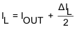
In addition, the inductor has to be rated for the appropriate saturation current and DC resistance (DCR). The inductor needs to be rated for a saturation current as high as the typical switch current limit of 5.5A or according to Equation 6 and Equation 7. Equation 6 and Equation 7 calculate the maximum inductor current under static load conditions. The formula takes the converter efficiency into account. The converter efficiency can be taken from the data sheet graphs or 80% can be used as a conservative approach. The calculation must be done for the maximum input voltage where the peak switch current is highest.
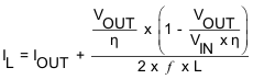
where
ƒ = Converter switching frequency (typically 1.4MHz)
L = Inductor value
η = Estimated converter efficiency (use the number from the efficiency curves or 0.80 as a conservative assumption)
Note: The calculation must be done for the maximum input voltage of the application
Calculating the maximum inductor current using the actual operating conditions gives the minimum saturation current. A margin of 20% should be added to cover for load transients during operation.
8.2.1.2.3 Input and Output Capacitor Selection
For best output and input voltage filtering, low ESR ceramic capacitors are recommended. The input capacitor minimizes input voltage ripple, suppresses input voltage spikes and provides a stable system rail for the device. A 22µF or larger input capacitor is required. The output capacitor value can range from 2x22µF up to 150µF. The recommended typical output capacitor value is 2x22µF and can vary over a wide range as outline in the output filter selection table.
8.2.1.2.4 Setting the Output Voltage
The output voltage is set by an external resistor divider according to the following equations:
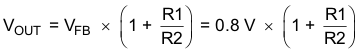
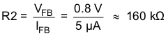
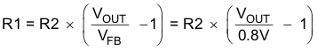
When sizing R2, in order to achieve low quiescent current and acceptable noise sensitivity, use a minimum of 5µA for the feedback current IFB. Larger currents through R2 improve noise sensitivity and output voltage accuracy.
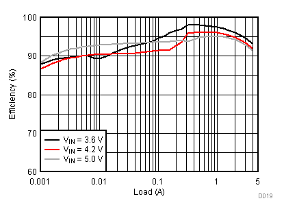
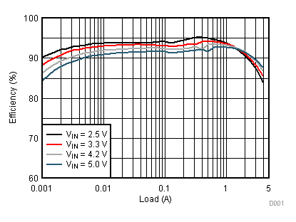
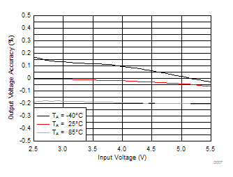
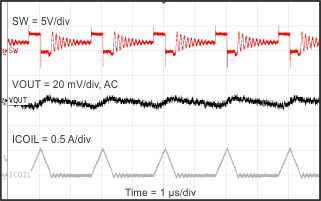
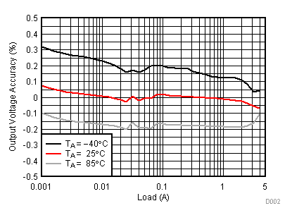
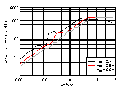
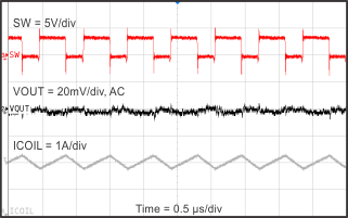
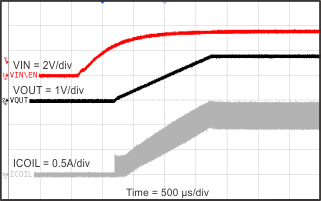
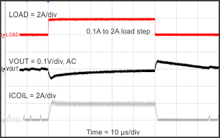
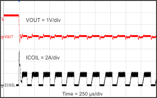
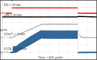
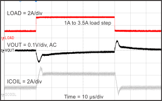
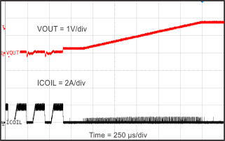
8.2.1.3 Application Performance Curves
TA = 25°C, VIN = 3.6V, VOUT = 1.8V, L1 = 1µH (XAL4020-102), C2 = 2x22µF, unless otherwise noted.
8.2.2 2.5V to 5.5V Input, 1.2V Output Converter

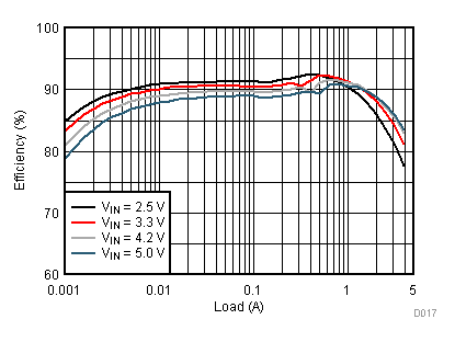 Figure 21. 1.2V Output Application Efficiency
8.2.3 3.0V to 5.5V Input, 2.6V Output Converter
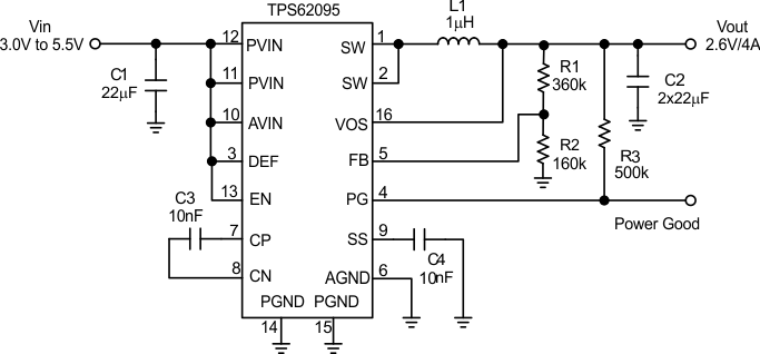
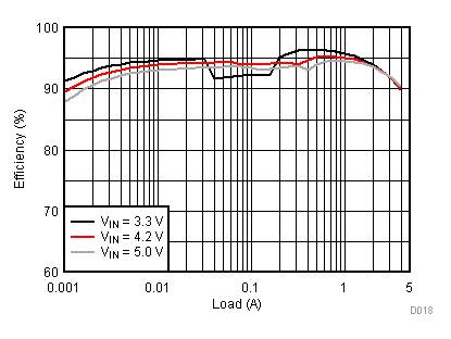 Figure 23. 2.6V Output Application Efficiency
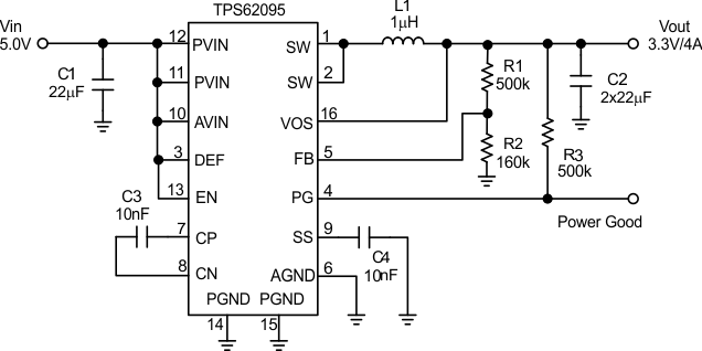
8.2.4 5V Input, 3.3V Output Converter