SLVSBD8A April 2014 – May 2014 TPS62095
PRODUCTION DATA.
- 1 Features
- 2 Applications
- 3 Description
- 4 Revision History
- 5 Pin Configuration and Functions
- 6 Specifications
- 7 Detailed Description
- 8 Application and Implementation
- 9 Power Supply Recommendations
- 10Layout
- 11Device and Documentation Support
- 12Mechanical, Packaging, and Orderable Information
パッケージ・オプション
メカニカル・データ(パッケージ|ピン)
- RGT|16
サーマルパッド・メカニカル・データ
- RGT|16
発注情報
7 Detailed Description
7.1 Overview
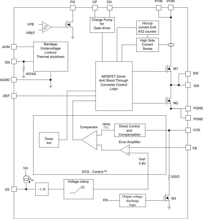
The TPS62095 synchronous step down converter is based on DCS-Control™ (Direct Control with Seamless transition into Power Save Mode). This is an advanced regulation topology that combines the advantages of hysteretic and voltage mode control.
The DCS-Control™ topology operates in PWM (Pulse Width Modulation) mode for medium to heavy load conditions and in Power Save Mode at light load currents. In PWM, the converter operates with its nominal switching frequency of 1.4 MHz having a controlled frequency variation over the input voltage range. As the load current decreases, the converter enters Power Save Mode, reducing the switching frequency and minimizing the IC's quiescent current to achieve high efficiency over the entire load current range. DCS-Control™ supports both operation modes using a single building block and therefore has a seamless transition from PWM to Power Save Mode without effects on the output voltage. The TPS62095 offers excellent DC voltage regulation and load transient regulation, combined with low output voltage ripple, minimizing interference with RF circuits.
7.2 Functional Block Diagram
7.3 Feature Description
7.3.1 PWM Operation
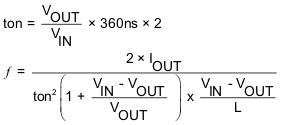
In PWM mode, the device operates with a fixed ON-time switching pulse at medium to heavy load currents. A quasi fixed switching frequency of typical 1.4MHz over the input and output voltage range is achieved by using an input feed forward. The ON-time is calculated as shown in Equation 2. As the load current decreases, the converter enters Power Save Mode operation reducing its switching frequency. The device enters Power Save Mode at the boundary to discontinuous conduction mode (DCM).
7.3.2 Low Dropout Operation (100% Duty Cycle)
The device offers low input to output voltage difference by entering 100% duty cycle mode. In this mode the high side MOSFET switch is constantly turned on. This is particularly useful in battery powered applications to achieve longest operation time by taking full advantage of the whole battery voltage range. The minimum input voltage where the output voltage falls below set point is given by:
Where
RDS(on) = High side FET on-resistance
RL = DC resistance of the inductor
VOUT(min) = Minimum output voltage the load can accept
7.3.3 Power Save Mode Operation
As the load current decreases, the converter enters Power Save Mode operation. During Power Save Mode, the converter operates with reduced switching frequency and with a minimum quiescent current to maintain high efficiency. The Power Save Mode is based on a fixed on-time architecture following Equation 2.
In Power Save Mode, the output voltage rises slightly above the nominal output voltage in PWM mode. This effect is reduced by increasing the output capacitance or the inductor value. This effect is also reduced by programming the output voltage of the TPS62095 lower than the target value. As an example, if the target output voltage is 3.3V, then the TPS62095 can be programmed to 3.3V - 0.3%. As a result, the output voltage accuracy is now -1.7% to +1.7% instead of -1.4% to 2%. The output voltage accuracy in PFM operation is reflected in the electrical specification table and given for a 2 x 22µF output capacitance.
7.4 Device Functional Modes
7.4.1 Soft Startup
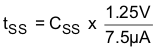
To minimize inrush current during startup, the device has an adjustable startup time depending on the capacitor value connected to the SS pin. The device charges the SS capacitor with a constant current of typically 7.5µA. The feedback voltage follows this voltage divided by 1.56, until the internal reference voltage of 0.8V is reached. The soft startup operation is completed once the voltage at the SS capacitor has reached typically 1.25V. The soft startup time is calculated using Equation 3. The larger the SS capacitor, the longer the soft startup time. The relation between the SS pin voltage and the FB pin voltage is estimated using Equation 4. Leaving the SS pin floating sets the minimum startup time.

During startup the switch current limit is reduced to 1/3 of its typical current limit of 5.5A when the output voltage is less than 0.6V. Once the output voltage exceeds typically 0.6V, the switch current limit is released to its nominal value. Thus, the device provides a reduced load current of 1.8A when the output voltage is below 0.6V. A small or no soft startup time may trigger this reduced switch current limit during startup, especially for larger output capacitor applications. This is avoided by using a larger soft start up capacitance which extends the soft startup time. See Short Circuit Protection (Hiccup-Mode) for details of the reduced current limit during startup.
7.4.2 Voltage Tracking
The SS pin can also be used to implement output voltage tracking with other supply rails, as shown in Figure 5.
In voltage tracking applications, the resistance R4 should be set properly to achieve accurate voltage tracking by taking 7.5μA soft startup current into account. 4.3kΩ is a sufficient value for R4. The relationship between V1 and V2 is shown in Equation 5. To achieve V1 startup leading V2, as shown in Figure 6, Equation 5 should be less than 1. To achieve simultaneous tracking, Equation 5 should equal to 1.
7.4.3 Short Circuit Protection (Hiccup-Mode)
The device is protected against hard short circuits to GND and over-current events. This is implemented by a two level short circuit protection. During start-up and when the output is shorted to GND, the switch current limit is reduced to 1/3 of its typical current limit of 5.5A. Once the output voltage exceeds typically 0.6V the current limit is released to its nominal value. The full current limit is implemented as a hiccup current limit. Once the internal current limit is triggered 32 times, the device stops switching and starts a new start-up sequence after a typical delay time of 66µS passed by. The device repeats these cycles until the high current condition is released.
7.4.4 Output Discharge Function
To make sure the device starts up under defined conditions, the output gets discharged via the VOS pin with a typical discharge resistor of 200Ω whenever the device shuts down. This happens when the device is disabled or if thermal shutdown, undervoltage lockout or short circuit hiccup-mode is triggered.
7.4.5 Power Good Output
The power good output is low when the output voltage is below its nominal value. The power good becomes high impedance once the output is within 5% of regulation. The PG pin is an open drain output and is specified to sink up to 1mA. This output requires a pull-up resistor to be monitored properly. The pull-up resistor cannot be connected to any voltage higher than the input voltage of the device.
7.4.6 Undervoltage Lockout
To avoid mis-operation of the device at low input voltages, an undervoltage lockout is included. UVLO shuts down the device at input voltages lower than typically 2.2V with a 200mV hysteresis.
7.4.7 Thermal Shutdown
The device goes into thermal shutdown once the junction temperature exceeds typically 150°C with a 20°C hysteresis.