SLVSBD8A April 2014 – May 2014 TPS62095
PRODUCTION DATA.
- 1 Features
- 2 Applications
- 3 Description
- 4 Revision History
- 5 Pin Configuration and Functions
- 6 Specifications
- 7 Detailed Description
- 8 Application and Implementation
- 9 Power Supply Recommendations
- 10Layout
- 11Device and Documentation Support
- 12Mechanical, Packaging, and Orderable Information
パッケージ・オプション
メカニカル・データ(パッケージ|ピン)
- RGT|16
サーマルパッド・メカニカル・データ
- RGT|16
発注情報
10 Layout
10.1 Layout Guidelines
- It is recommended to place all components as close as possible to the IC. Specially, the input capacitor placement is closest to the PVIN and PGND pins of the device.
- Use wide and short traces for the main current paths to reduce the parasitic inductance and resistance, like the SW node.
- The VOS pin is noise sensitive and needs to be routed as short and directly to the output pin of the inductor and the output capacitor. This minimizes switch node jitter.
- The exposed thermal pad of the package, the AGND and the PGND should have a single joint connection at the exposed thermal pad of the package. To enhance heat dissipation of the device, the exposed thermal pad should be connected to bottom or internal layer ground planes using vias.
- The charge pump capacitor connected to CP and CN should be placed close to the IC to minimize coupling of switching waveforms into other traces and circuits.
- The capacitor on the SS pin and the FB resistors divider network should be placed close to the IC and connected directly to those pins and the AGND pin.
- Refer to Figure 26 for an example of component placement, routing and thermal design.
10.2 Layout Example
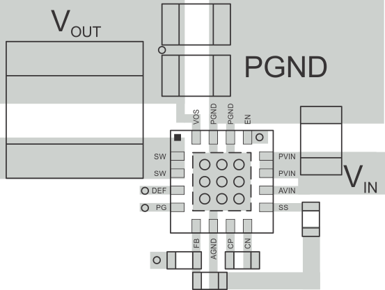 Figure 26. TPS62095 PCB Layout
10.3 Thermal Consideration
Implementation of integrated circuits in low-profile and fine-pitch surface-mount packages typically requires special attention to power dissipation. Many system-dependent issues such as thermal coupling, airflow, added heat sinks and convection surfaces, and the presence of other heat-generating components affect the power-dissipation limits of a given component. The Thermal Information table provides the thermal metric of the device and its package based on JEDEC standard. For more details on how to use the thermal parameters in real applications, see the application notes: SZZA017 and SPRA953.