SLVSBD8A April 2014 – May 2014 TPS62095
PRODUCTION DATA.
- 1 Features
- 2 Applications
- 3 Description
- 4 Revision History
- 5 Pin Configuration and Functions
- 6 Specifications
- 7 Detailed Description
- 8 Application and Implementation
- 9 Power Supply Recommendations
- 10Layout
- 11Device and Documentation Support
- 12Mechanical, Packaging, and Orderable Information
パッケージ・オプション
メカニカル・データ(パッケージ|ピン)
- RGT|16
サーマルパッド・メカニカル・データ
- RGT|16
発注情報
5 Pin Configuration and Functions
16-Pin VQFN with Thermal PAD
RGT
(Top View)
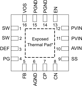
Pin Functions
| PIN | DESCRIPTION | |
|---|---|---|
| NAME | NO. | |
| SW | 1, 2 | Switch pin of the power stage. |
| DEF | 3 | This pin is used for internal logic and needs to be pulled high. This pin must be connected to the AVIN pin. |
| PG | 4 | Power good open drain output. A pull up resistor can not be connected to any voltage higher than the input voltage. |
| FB | 5 | Feedback pin, for regulating the output voltage. |
| AGND | 6 | Analog ground. |
| CP | 7 | Internal charge pump's flying capacitor. Connect a 10nF capacitor between CP and CN. |
| CN | 8 | Internal charge pump's flying capacitor. Connect a 10nF capacitor between CP and CN. |
| SS | 9 | Soft-start control pin. A capacitor is connected to this pin and sets the soft startup time. Leaving this pin floating sets the minimum start-up time. |
| AVIN | 10 | Analog supply input voltage pin. |
| PVIN | 11,12 | Power supply input voltage pin. |
| EN | 13 | Enable pin. This pin has an active pull down resistor of typically 400kΩ. |
| PGND | 14,15 | Power ground. |
| VOS | 16 | Output voltage sense pin. This pin must be directly connected to the output voltage. |
| Thermal Pad | The exposed thermal pad must be connected to AGND. | |