JAJSBR8E March 2012 – May 2017 TPS62125
PRODUCTION DATA.
- 1 特長
- 2 アプリケーション
- 3 概要
- 4 改訂履歴
- 5 Pin Configuration and Functions
- 6 Specifications
- 7 Detailed Description
- 8 Application and Implementation
- 9 Power Supply Recommendations
- 10Layout
- 11デバイスおよびドキュメントのサポート
- 12メカニカル、パッケージ、および注文情報
パッケージ・オプション
メカニカル・データ(パッケージ|ピン)
- DSG|8
サーマルパッド・メカニカル・データ
- DSG|8
発注情報
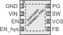
5 Pin Configuration and Functions
DSG Package
8-Pin WSON
Top View

Pin Functions
| PIN | I/O | DESCRIPTION | ||
|---|---|---|---|---|
| NAME | NO. | |||
| EN | 3 | IN | Input pin for the enable comparator. Pulling this pin to GND turns the device into shutdown mode. The DC/DC converter is enabled once the rising voltage on this pin trips the enable comparator threshold, VTH EN ON of typ. 1.2 V. The DC/DC converter is turned off once a falling voltage on this pin trips the threshold, VTH EN OFF of typ. 1.15 V. The comparator threshold can be increased by connecting an external resistor to pin EN_hys. See also application section. This pin must be terminated. | |
| EN_hys | 4 | OUT | Enable hysteresis open-drain output. This pin is pulled to GND when the voltage on the EN pin is below the comparator threshold VTH EN ON of typ. 1.2 V and the comparator has not yet tripped. The pin is high impedance once the enable comparator has tripped and the voltage at the pin EN is above the threshold VTH EN ON. The pin is pulled to GND once the falling voltage on the EN pin trips the threshold VTH EN OFF (1.15 V typical). This pin can be used to increase the hysteresis of the enable comparator. If not used, tie this pin to GND, or leave it open. | |
| FB | 5 | IN | This is the feedback pin for the regulator. An external resistor divider network connected to this pin sets the output voltage. In case of fixed output voltage option, the resistor divider is integrated and the pin need to be connected directly to the output voltage. | |
| GND | 1 | PWR | GND supply pin. | |
| PG | 8 | OUT | Open drain power good output. This pin is internally pulled to GND when the device is disabled or the output voltage is below the PG threshold. The pin is floating when the output voltage is in regulation and above the PG threshold. For power good indication, the pin can be connected via a pull up resistor to a voltage rail up to 10 . The pin can sink a current up to 0.4 mA and maintain the specified high/low voltage levels. It can be used to discharge the output capacitor with up to 10 mA. In this case the current into the pin must be limited with an appropriate pull up resistor. More details can be found in the application section. If not used, leave the pin open, or connect to GND. | |
| SW | 7 | OUT | This is the switch pin and is connected to the internal MOSFET switches. Connect the inductor to this pin. Do not tie this pin to VIN, VOUT or GND. | |
| VIN | 2 | PWR | VIN power supply pin. | |
| VOS | 6 | IN | This is the output voltage sense pin for the DCS-Control circuitry. This pin must be connected to the output voltage of the DC/DC converter. | |
| Exposed Thermal PAD | – | – | This pad must be connected to GND. | |