JAJSBI2F November 2011 – November 2021 TPS62130 , TPS62130A , TPS62131 , TPS62132 , TPS62133
PRODUCTION DATA
- 1 特長
- 2 アプリケーション
- 3 概要
- 4 Revision History
- 5 Device Comparison Table
- 6 Pin Configuration and Functions
- 7 Specifications
- 8 Detailed Description
- 9 Application and Implementation
- 10Power Supply Recommendations
- 11Layout
- 12Device and Documentation Support
- 13Mechanical, Packaging, and Orderable Information
パッケージ・オプション
メカニカル・データ(パッケージ|ピン)
- RGT|16
サーマルパッド・メカニカル・データ
- RGT|16
発注情報
9.2.2.3 Tracking Function
If a tracking function is desired, the SS/TR pin can be used for this purpose by connecting it to an external tracking voltage. The output voltage tracks that voltage. If the tracking voltage is between 50 mV and 1.2 V, the FB pin will track the SS/TR pin voltage as described in Equation 11 and shown in Figure 9-2.
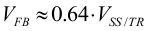
 Figure 9-2 Voltage Tracking Relationship
Once the SS/TR pin voltage reaches approximately 1.2 V, the internal voltage is clamped to the internal feedback voltage and device goes to normal regulation. This works for rising and falling tracking voltages with the same behavior, as long as the input voltage is inside the recommended operating conditions. For decreasing SS/TR pin voltage, the device does not sink current from the output. So, the resulting decrease of the output voltage can be slower than the SS/TR pin voltage if the load is light. When driving the SS/TR pin with an external voltage, do not exceed the voltage rating of the SS/TR pin which is VIN + 0.3 V.
If the input voltage drops into undervoltage lockout or even down to zero, the output voltage will go to zero, independent of the tracking voltage. Figure 9-3 shows how to connect devices to get ratiometric and simultaneous sequencing by using the tracking function.
 Figure 9-3 Sequence For Ratiometric
And Simultaneous Start-Up
Figure 9-3 Sequence For Ratiometric
And Simultaneous Start-UpThe resistive divider of R1 and R2 can be used to change the ramp rate of VOUT2 faster, slower, or the same as VOUT1.
A sequential start-up is achieved by connecting the PG pin of VOUT1 to the EN pin of VOUT2. A ratiometric start-up sequence happens if both supplies are sharing the same soft-start capacitor. Equation 10 calculates the soft-start time, though the SS/TR current has to be doubled. Details about these and other tracking and sequencing circuits are found in Sequencing and Tracking With the TPS621-Family and TPS821-Family Application Report.