JAJSBI2F November   2011  – November 2021 TPS62130 , TPS62130A , TPS62131 , TPS62132 , TPS62133

PRODUCTION DATA  

  1. 特長
  2. アプリケーション
  3. 概要
  4. Revision History
  5. Device Comparison Table
  6. Pin Configuration and Functions
  7. Specifications
    1. 7.1 Absolute Maximum Ratings (1)
    2. 7.2 ESD Ratings
    3. 7.3 Recommended Operating Conditions
    4. 7.4 Thermal Information
    5. 7.5 Electrical Characteristics
    6. 7.6 Typical Characteristics
  8. Detailed Description
    1. 8.1 Overview
    2. 8.2 Functional Block Diagram
    3. 8.3 Feature Description
      1. 8.3.1 Enable / Shutdown (EN)
      2. 8.3.2 Soft Start / Tracking (SS/TR)
      3. 8.3.3 Power Good (PG)
      4. 8.3.4 Pin-Selectable Output Voltage (DEF)
      5. 8.3.5 Frequency Selection (FSW)
      6. 8.3.6 Undervoltage Lockout (UVLO)
      7. 8.3.7 Thermal Shutdown
    4. 8.4 Device Functional Modes
      1. 8.4.1 Pulse Width Modulation (PWM) Operation
      2. 8.4.2 Power Save Mode Operation
      3. 8.4.3 100% Duty-Cycle Operation
      4. 8.4.4 Current Limit And Short Circuit Protection
  9. Application and Implementation
    1. 9.1 Application Information
    2. 9.2 Typical Application
      1. 9.2.1 Design Requirements
      2. 9.2.2 Detailed Design Procedure
        1. 9.2.2.1 Programming The Output Voltage
        2. 9.2.2.2 External Component Selection
          1. 9.2.2.2.1 Inductor Selection
          2. 9.2.2.2.2 Capacitor Selection
            1. 9.2.2.2.2.1 Output Capacitor
            2. 9.2.2.2.2.2 Input Capacitor
            3. 9.2.2.2.2.3 Soft-Start Capacitor
        3. 9.2.2.3 Tracking Function
        4. 9.2.2.4 Output Filter And Loop Stability
      3. 9.2.3 Application Curves
    3. 9.3 System Examples
      1. 9.3.1 LED Power Supply
      2. 9.3.2 Active Output Discharge
      3. 9.3.3 –3.3-V Inverting Power Supply
      4. 9.3.4 Various Output Voltages
  10. 10Power Supply Recommendations
  11. 11Layout
    1. 11.1 Layout Guidelines
    2. 11.2 Layout Example
    3. 11.3 Thermal Information
  12. 12Device and Documentation Support
    1. 12.1 Device Support
      1. 12.1.1 Third-Party Products Disclaimer
    2. 12.2 Documentation Support
      1. 12.2.1 Related Documentation
    3. 12.3 Receiving Notification of Documentation Updates
    4. 12.4 サポート・リソース
    5. 12.5 Trademarks
    6. 12.6 Electrostatic Discharge Caution
    7. 12.7 Glossary
  13. 13Mechanical, Packaging, and Orderable Information

パッケージ・オプション

メカニカル・データ(パッケージ|ピン)
サーマルパッド・メカニカル・データ
発注情報

LED Power Supply

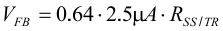
The TPS62130 can be used as a power supply for power LEDs. The FB pin can be easily set down to lower values than nominal by using the SS/TR pin. With that, the voltage drop on the sense resistor is low to avoid excessive power loss. Since this pin provides 2.5 µA, the feedback pin voltage can be adjusted by an external resistor per Equation 15. This drop, proportional to the LED current, is used to regulate the output voltage (anode voltage) to a proper level to drive the LED. Both analog and PWM dimming are supported with the TPS62130. Figure 9-40 shows an application circuit, tested with analog dimming:

GUID-D8E9E2FC-C24F-457D-8518-F5970D98211A-low.gifFigure 9-40 Single Power LED Supply

The resistor at SS/TR sets the FB voltage to a level of approximately 300 mV and is calculated from Equation 15.

Equation 15. GUID-429B0A4D-5781-4D80-9AFF-C7B4BAAC8B73-low.gif

The device now supplies a constant current, set by the resistor at the FB pin, by regulating the output voltage accordingly. The minimum input voltage has to be rated according the forward voltage needed by the LED used. More information is available in the Step-Down LED Driver With Dimming With the TPS621-Family and TPS821-Family Application Report.