JAJSBI2F November   2011  – November 2021 TPS62130 , TPS62130A , TPS62131 , TPS62132 , TPS62133

PRODUCTION DATA  

  1. 特長
  2. アプリケーション
  3. 概要
  4. Revision History
  5. Device Comparison Table
  6. Pin Configuration and Functions
  7. Specifications
    1. 7.1 Absolute Maximum Ratings (1)
    2. 7.2 ESD Ratings
    3. 7.3 Recommended Operating Conditions
    4. 7.4 Thermal Information
    5. 7.5 Electrical Characteristics
    6. 7.6 Typical Characteristics
  8. Detailed Description
    1. 8.1 Overview
    2. 8.2 Functional Block Diagram
    3. 8.3 Feature Description
      1. 8.3.1 Enable / Shutdown (EN)
      2. 8.3.2 Soft Start / Tracking (SS/TR)
      3. 8.3.3 Power Good (PG)
      4. 8.3.4 Pin-Selectable Output Voltage (DEF)
      5. 8.3.5 Frequency Selection (FSW)
      6. 8.3.6 Undervoltage Lockout (UVLO)
      7. 8.3.7 Thermal Shutdown
    4. 8.4 Device Functional Modes
      1. 8.4.1 Pulse Width Modulation (PWM) Operation
      2. 8.4.2 Power Save Mode Operation
      3. 8.4.3 100% Duty-Cycle Operation
      4. 8.4.4 Current Limit And Short Circuit Protection
  9. Application and Implementation
    1. 9.1 Application Information
    2. 9.2 Typical Application
      1. 9.2.1 Design Requirements
      2. 9.2.2 Detailed Design Procedure
        1. 9.2.2.1 Programming The Output Voltage
        2. 9.2.2.2 External Component Selection
          1. 9.2.2.2.1 Inductor Selection
          2. 9.2.2.2.2 Capacitor Selection
            1. 9.2.2.2.2.1 Output Capacitor
            2. 9.2.2.2.2.2 Input Capacitor
            3. 9.2.2.2.2.3 Soft-Start Capacitor
        3. 9.2.2.3 Tracking Function
        4. 9.2.2.4 Output Filter And Loop Stability
      3. 9.2.3 Application Curves
    3. 9.3 System Examples
      1. 9.3.1 LED Power Supply
      2. 9.3.2 Active Output Discharge
      3. 9.3.3 –3.3-V Inverting Power Supply
      4. 9.3.4 Various Output Voltages
  10. 10Power Supply Recommendations
  11. 11Layout
    1. 11.1 Layout Guidelines
    2. 11.2 Layout Example
    3. 11.3 Thermal Information
  12. 12Device and Documentation Support
    1. 12.1 Device Support
      1. 12.1.1 Third-Party Products Disclaimer
    2. 12.2 Documentation Support
      1. 12.2.1 Related Documentation
    3. 12.3 Receiving Notification of Documentation Updates
    4. 12.4 サポート・リソース
    5. 12.5 Trademarks
    6. 12.6 Electrostatic Discharge Caution
    7. 12.7 Glossary
  13. 13Mechanical, Packaging, and Orderable Information

パッケージ・オプション

メカニカル・データ(パッケージ|ピン)
サーマルパッド・メカニカル・データ
発注情報

Current Limit And Short Circuit Protection

The TPS6213x devices have protection against heavy load and short circuit events. If a short circuit is detected (VOUT drops below 0.5 V), the current limit is reduced to 1.6 A typically. If the output voltage rises above 0.5 V, the device runs in normal operation again. At heavy loads, the current limit determines the maximum output current. If the current limit is reached, the high-side FET is turned off. Avoiding shoot-through current, then the low-side FET switches on to allow the inductor current to decrease. The low-side current limit is typically 3.5 A. The high-side FET turns on again only if the current in the low-side FET has decreased below the low-side current limit threshold.

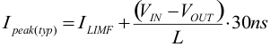
The output current of the device is limited by the current limit. Due to internal propagation delay, the actual current can exceed the static current limit during that time. The dynamic current limit can be calculated as follows:
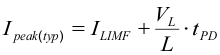
Equation 4. GUID-3FD4CFE7-8ADF-4DF9-BBB2-662040D73C50-low.gif

where

  • ILIMF is the static current limit, specified in the Electrical Characteristics.
  • L is the inductor value.
  • VL is the voltage across the inductor (VIN - VOUT).
  • tPD is the internal propagation delay.

The current limit can exceed static values, especially if the input voltage is high and very small inductances are used. The dynamic high-side switch peak current can be calculated as follows:

Equation 5. GUID-9E31BDFC-9FA1-4128-A858-B43F25FA2AFF-low.gif