SLVSB02B November 2013 – July 2014 TPS62740 , TPS62742
PRODUCTION DATA.
- 1 Features
- 2 Applications
- 3 Description
- 4 Revision History
- 5 Device Comparison Table
- 6 Specifications
- 7 Detailed Description
- 8 Application and Implementation
- 9 Power Supply Recommendations
- 10Layout
- 11Device and Documentation Support
- 12Mechanical, Packaging, and Orderable Information
パッケージ・オプション
メカニカル・データ(パッケージ|ピン)
- DSS|12
サーマルパッド・メカニカル・データ
- DSS|12
発注情報
6 Specifications
6.1 Absolute Maximum Ratings(1)
Over operating free-air temperature range (unless otherwise noted)| MIN | MAX | UNIT | |||
|---|---|---|---|---|---|
| Pin voltage(2) | VIN | –0.3 | 6 | V | |
| SW (3) | –0.3 | VIN +0.3V | V | ||
| EN, CTRL, VSEL1-4 | –0.3 | VIN +0.3V | V | ||
| PG | –0.3 | VIN +0.3V | V | ||
| VOUT, LOAD | –0.3 | 3.7 | V | ||
| PG pin | IPG | sink current | 10 | mA | |
| Maximum operating junction temperature, TJ | –40 | 150 | °C | ||
(1) Stresses beyond those listed under absolute maximum ratings may cause permanent damage to the device. These are stress ratings only and functional operation of the device at these or any other conditions beyond those indicated under recommended operating conditions is not implied. Exposure to absolute–maximum–rated conditions for extended periods may affect device reliability.
(2) All voltage values are with respect to network ground terminal GND.
(3) The MAX value VIN +0.3V applies for applicative operation (device switching), DC voltage applied to this pin may not exceed 4V
6.2 Handling Ratings
| MIN | MAX | UNIT | |||
|---|---|---|---|---|---|
| Tstg | Storage temperature range | –65 | 150 | °C | |
| V(ESD) | Electrostatic discharge | Human body model (HBM), per ANSI/ESDA/JEDEC JS-001, all pins(1) | 2000 | V | |
| Charged device model (CDM), per JEDEC specification JESD22-C101, all pins(2) | 1000 | ||||
(1) JEDEC document JEP155 states that 500-V HBM allows safe manufacturing with a standard ESD control process. The human body model is a 100-pF capacitor discharged through a 1.5-kΩ resistor into each pin.
(2) JEDEC document JEP157 states that 250-V CDM allows safe manufacturing with a standard ESD control process.
6.3 Recommended Operating Conditions
| MIN | NOM | MAX | UNIT | ||||||
|---|---|---|---|---|---|---|---|---|---|
| VIN | Supply voltage VIN(1) | 2.2 | 5.5 | V | |||||
| IOUT + I LOAD | Device output current (sum of IOUT and I LOAD) | VOUTnom + 0.7V ≤ VIN ≤ 5.5V | TPS62740 | 300 | mA | ||||
| 3V ≤ VIN, VOUTnom + 0.7V ≤ VIN ≤ 5.5V | TPS62742 | 400 | |||||||
| VOUTnom ≤ VIN ≤ VOUTnom +0.7V | 100 | ||||||||
| ILOAD | Load current (current from LOAD pin) | 100 | |||||||
| L | Inductance | 1.5 | 2.2 | 3.3 | µH | ||||
| COUT | Output capacitance connected to VOUT pin (not including LOAD pin) | 22 | µF | ||||||
| CLOAD | Capacitance connected to LOAD pin | 10 | |||||||
| TJ | Operating junction temperature range | -40 | 125 | °C | |||||
| TA | Ambient temperature range | -40 | 85 | ||||||
(1) The minimum required supply voltage for startup is 2.15V (undervoltage lockout threshold VTH_UVLO+) . The device is functional down to 2V supply voltage (falling undervoltage lockout threshold VTH_UVLO-).
6.4 Thermal Information
| THERMAL METRIC | DSS / 12 PINS | UNIT | |
|---|---|---|---|
| RθJA | Junction-to-ambient thermal resistance | 61.8 | °C/W |
| RθJCtop | Junction-to-case (top) thermal resistance | 70.9 | |
| RθJB | Junction-to-board thermal resistance | 25.7 | |
| ψJT | Junction-to-top characterization parameter | 1.9 | |
| ψJB | Junction-to-board characterization parameter | 25.7 | |
| RθJCbot | Junction-to-case (bottom) thermal resistance | 7.2 | |
6.5 Electrical Characteristics
VIN = 3.6V, TA = –40°C to 85°C typical values are at TA = 25°C (unless otherwise noted)| PARAMETER | TEST CONDITIONS | MIN | TYP | MAX | UNIT | |||
|---|---|---|---|---|---|---|---|---|
| SUPPLY | ||||||||
| VIN | Input voltage range | 2.2 | 5.5 | V | ||||
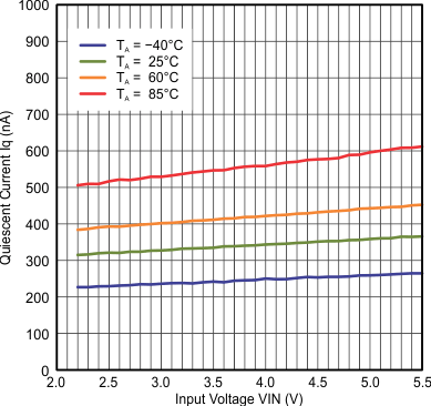
| IQ | Operating quiescent current | EN = VIN, CTRL = GND, IOUT = 0µA, VOUT = 1.8V, device not switching, | 360 | 1800 | nA | |||
| EN = VIN, IOUT = 0mA, CTRL = GND, VOUT = 1.8V , device switching | 460 | |||||||
| EN = VIN, IOUT = 0mA., CTRL = VIN, VOUT = 1.8V, device not switching | 12.5 | µA | ||||||
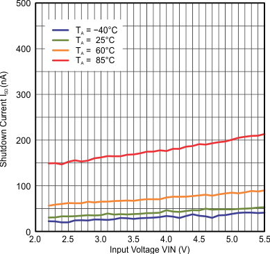
| ISD | Shutdown current | EN = GND, shutdown current into VIN | 70 | 1000 | nA | |||
| EN = GND, shutdown current into VIN, TA = 60°C | 150 | 450 | ||||||
| VTH_UVLO+ | Undervoltage lockout threshold | Rising VIN | 2.075 | 2.15 | V | |||
| VTH_UVLO- | Falling VIN | 1.925 | 2 | |||||
| INPUTS EN, CTRL, VSEL 1-4 | ||||||||
| VIH TH | High level input threshold | 2.2V ≤ VIN ≤ 5.5V | 1.1 | V | ||||
| VIL TH | Low level input threshold | 2.2V ≤ VIN ≤ 5.5V | 0.4 | V | ||||
| IIN | Input bias Current | TA = 25°C | 10 | nA | ||||
| TA = –40°C to 85°C | 25 | |||||||
| POWER SWITCHES | ||||||||
| RDS(ON) | High side MOSFET on-resistance | VIN = 3.6V, IOUT = 50mA | 0.6 | 0.85 | Ω | |||
| Low Side MOSFET on-resistance | 0.36 | 0.5 | ||||||
| ILIMF | High side MOSFET switch current limit | 2.2V ≤ VIN ≤ 5.5V, TPS62740 | 480 | 600 | 720 | mA | ||
| 3.0V ≤ VIN ≤ 5.5V, TPS62742 | 590 | 650 | 740 | |||||
| Low side MOSFET switch current limit | TPS62740 | 600 | mA | |||||
| TPS62742 | 650 | |||||||
| OUTPUT DISCHARGE SWITCH (VOUT) | ||||||||
| RDSCH_VOUT | MOSFET on-resistance | VIN = 3.6V, EN = GND, IOUT = -10mA into VOUT pin | 30 | 65 | Ω | |||
| IIN_VOUT | Bias current into VOUT pin | VIN = 3.6V, EN = VIN, VOUT = 2V, CTRL = GND | TA = 25°C | 40 | 100 | nA | ||
| TA = –40°C to 85°C | 1010 | |||||||
| LOAD OUTPUT (LOAD) | ||||||||
| RLOAD | High side MOSFET on-resistance | ILOAD = 50mA, CTRL = VIN, VOUT = 2.0V, 2.2 V ≤ VIN ≤ 5.5V | 0.6 | 1.25 | Ω | |||
| RDSCH_LOAD | Low side MOSFET on-resistance | CTRL = GND, 2.2V ≤ VIN ≤ 5.5V, ILOAD = - 10mA | 30 | 65 | ||||
| tRise_LOAD | VLOAD rise time | Starting with CTRL low to high transition, time to ramp VLOAD from 0V to 95% VOUT = 1.8V, 2.2V ≤ VIN ≤ 5.5V, ILOAD = 1mA | 315 | 800 | µs | |||
| AUTO 100% MODE TRANSITION | ||||||||
| VTH_100+ | Auto 100% Mode leave detection threshold (1) | Rising VIN,100% Mode is left with VIN = VOUT + VTH_100+ , max value at TJ = 85°C | 170 | 250 | 340 | mV | ||
| VTH_100- | Auto 100% Mode enter detection threshold (1) | Falling VIN, 100% Mode is entered with VIN = VOUT + VTH_100-, max value at TJ = 85°C | 110 | 200 | 280 | |||
| POWER GOOD OUTPUT (PG, OPEN DRAIN) | ||||||||
| VTH_PG+ | Power good threshold voltage | Rising output voltage on VOUT pin, referred to VVOUT | 97.5% | |||||
| VPG_Hys | Hysteresis | -3% | ||||||
| VOL | Low level output voltage | 2.2V ≤ VIN ≤ 5.5V, EN = GND, current into PG pin IPG = 4mA | 0.3 | V | ||||
| IIN_PG | Bias current into PG pin | PG pin is high impedance, VOUT = 2V, EN = VIN, CTRL = GND, IOUT = 0mA | TA = 25°C | 0 | 10 | nA | ||
| TA = –40°C to 85°C | 25 | |||||||
| OUTPUT | ||||||||
| tONmin | Minimum ON time | VIN = 3.6V, VOUT = 2.0V, IOUT = 0 mA | 225 | ns | ||||
| tOFFmin | Minimum OFF time | VIN = 2.3V | 50 | ns | ||||
| tStartup_delay | Regulator start up delay time | VIN = 3.6V, from transition EN = low to high until device starts switching | 10 | 25 | ms | |||
| tSoftstart | Softstart time with reduced switch current limit | 2.2V ≤ VIN ≤ 5.5V, EN = VIN | 700 | 1200 | µs | |||
| ILIM_softstart | High side MOSFET switch current limit | Reduced switch current limit during softstart | TPS62740 | 80 | 150 | 200 | mA | |
| TPS62742 | 150 | |||||||
| Low side MOSFET switch current limit | 150 | |||||||
| VVOUT | Output voltage range | Output voltages are selected with pins VSEL 1 - 4 | 1.8 | 3.3 | V | |||
| Output voltage accuracy | VIN = 3.6V, IOUT = 10mA, VOUT = 1.8V | -2.5 | 0% | 2.5 | ||||
| VIN = 3.6V, IOUT = 100mA, VOUT = 1.8V | –2 | 0% | 2 | |||||
| DC output voltage load regulation | VOUT = 1.8V, VIN = 3.6V, CTRL = VIN | 0.001 | %/mA | |||||
| DC output voltage line regulation | VOUT = 1.8V, CTRL = VIN, IOUT = 10 mA, 2.5V ≤ VIN ≤ 5.5V | 0 | %/V | |||||
(1) VIN is compared to the programmed output voltage (VOUT). When VIN–VOUT falls below VTH_100- the device enters 100% Mode by turning the high side MOSFET on. The 100% Mode is exited when VIN–VOUT exceeds VTH_100+ and the device starts switching. The hysteresis for the 100% Mode detection threshold VTH_100+ - VTH_100- will always be positive and will be approximately 50 mV(typ.)
6.6 Typical Characteristics
| EN = VIN, VOUT = 1.8V, CTRL = GND | Device Not Switching | |
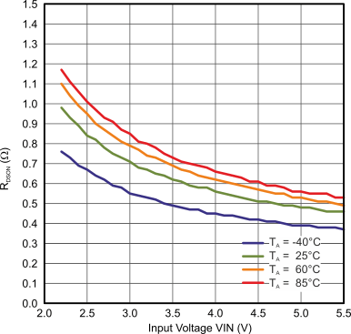 Figure 3. RDSON High Side Mosfet
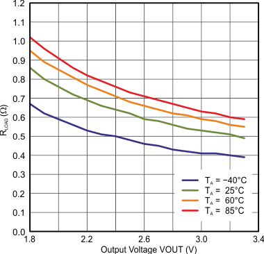 Figure 5. Load Switch Resistance RLOAD
| EN = GND |
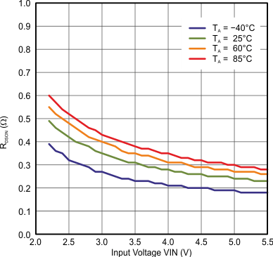 Figure 4. RDSON Low Side Mosfet