SLVS810C June 2009 – September 2015 TPS65000 , TPS650001 , TPS650003 , TPS650006 , TPS65001 , TPS650061
PRODUCTION DATA.
- 1 Features
- 2 Applications
- 3 Description
- 4 Revision History
- 5 Description (continued)
- 6 Device Options
- 7 Pin Configuration and Functions
- 8 Specifications
- 9 Detailed Description
- 10Application and Implementation
- 11Power Supply Recommendations
- 12Layout
- 13Device and Documentation Support
- 14Mechanical, Packaging, and Orderable Information
パッケージ・オプション
メカニカル・データ(パッケージ|ピン)
- RTE|16
サーマルパッド・メカニカル・データ
- RTE|16
発注情報
10 Application and Implementation
NOTE
Information in the following applications sections is not part of the TI-component specification, and TI does not warrant its accuracy or completeness. TI’s customers are responsible for determining suitability of components for their purposes. Customers should validate and test their design implementation to confirm system functionality.
10.1 Application Information
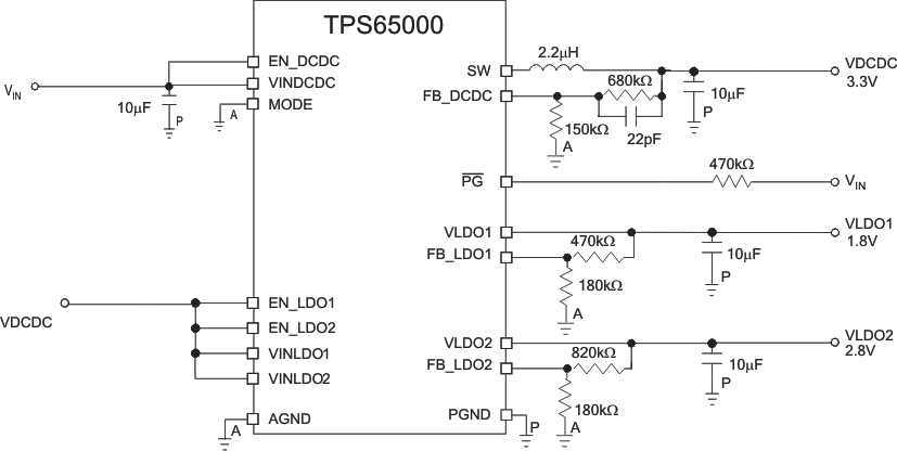
The TPS65000 device is designed to pair with various applications, such as embedded processor power and portable media players. For detailed information on using the TPS65000 with TMS32C2834x, see Related Documentation.
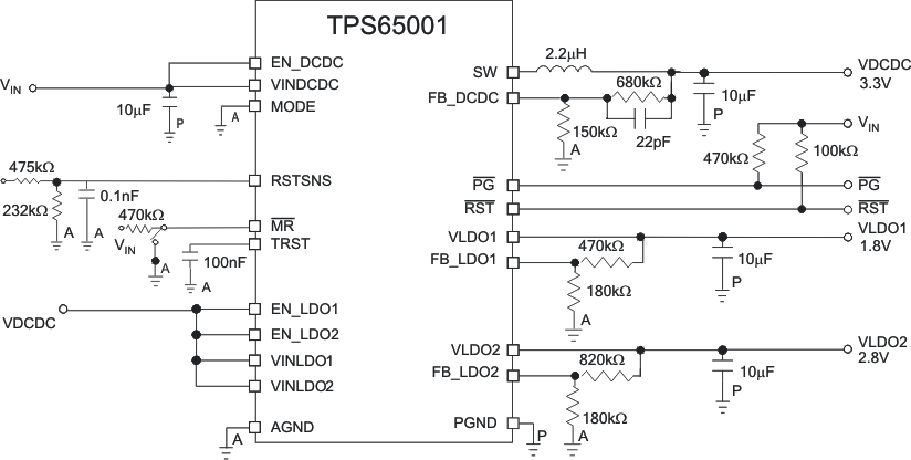
TI designed the TPS65001 device to pair with various applications, such as PDAs and pocket PCs. For detailed information on using the TPS65001 with TMS320C5504/05, see Related Documentation.
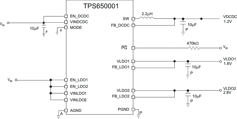
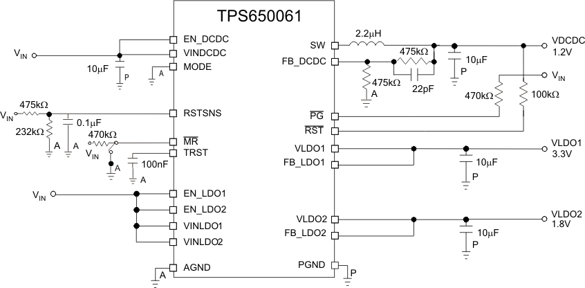
TI designed the TPS650001 and TPS650061 devices to pair with various applications, such as cell and smart phones, as well as point-of-load. For detailed information on using the TPS650001 and TPS650061 with OMAP-L13x, see Related Documentation.
10.2 Typical Application
10.2.1 Typical TPS65000 Application
10.2.1.1 Design Requirements
For this design example, use the parameters listed in Table 2.
Table 2. Design Parameters
| RESOURCES | VOLTAGE |
|---|---|
| SW | 3.3 V |
| VLDO1 | 1.8 V |
| VLDO2 | 2.8 V |
10.2.1.2 Detailed Design Procedure
10.2.1.2.1 Output Filter Design (Inductor and Output Capacitor)
10.2.1.2.1.1 Inductor Selection
The typical value for the converter inductor is 2.2-μH output inductor. Larger or smaller inductor values in the range of 1.5 μH to 3.3 μH can optimize the performance of the device for specific operation conditions. The selected inductor has to be rated for its DC resistance and saturation current. The DC resistance of the inductance influences the efficiency of the converter directly. An inductor with lowest DC resistance must be selected for highest efficiency. See SLVA157 for more information on inductor selection.
Equation 5 calculates the maximum inductor current under static load conditions. The saturation current of the inductor should be rated higher than the maximum inductor current as calculated with Equation 6. TI recommends this because during heavy load transient the inductor current rises above the calculated value.

where
- f = Switching Frequency (2.25 MHz typical)
- L = Inductor Value
- ΔIL = Peak to Peak Inductor Ripple Current

where
- ILmax = Maximum Inductor Current
The highest inductor current occurs at maximum VIN.
Open-core inductors have a soft saturation characteristic and can usually handle higher inductor currents versus a comparable shielded inductor.
A more conservative approach is to select the inductor current rating just for the maximum switch current of the corresponding converter. Consider that the core material from inductor to inductor differs and impacts the efficiency especially at high-switching frequencies.
The step down converter has internal loop compensation. TI designed the internal loop compensation to work with a certain output filter corner frequency calculated as follows:

The selection of external L-C filter must be coped with Equation 7. The product of L × COUT must be constant while selecting smaller inductor or increasing output capacitor value.
See Table 3 and the typical applications for possible inductors.
Table 3. Inductors
| INDUCTOR TYPE | INDUCTANCE (μH) | SUPPLIER | MAX DIMENSIONS (mm) |
|---|---|---|---|
| MIPS2520D2R2 | 2.0 | FDK | 2.5 × 2.0 × 1.0 |
| MIPSA2520D2R2 | 2.0 | FDK | 2.5 × 2.0 × 1.2 |
| KSLI-252010AG2R2 | 2.2 | Htachi Metals | 2.5 × 2.0 × 1.0 |
| LQM2HPN2R2MJ0L | 2.2 | Murata | 2.5 × 2.0 × 1.2 |
| LPS15222 | 2.2 | Coilcraft | 3.0 × 3.0 × 1.5 |
10.2.1.2.1.2 Output Capacitor Selection
The advanced fast response voltage mode control scheme of the converter allows the use of small ceramic capacitors with a typical value of 22 μF, without having large output voltage under and overshoots during heavy load transients. TI recommends ceramic capacitors with low ESR values because they result in lowest output voltage ripple. See the TI-recommended components.
If ceramic output capacitors are used, the capacitor RMS ripple current rating always meets the application requirements. The RMS ripple current is calculated as the following:

At nominal load current, the device operates in PWM mode and the overall output voltage ripple is the sum of the voltage spike caused by the output capacitor ESR plus the voltage ripple caused by charging and discharging the output capacitor:

Where the highest output voltage ripple occurs at the highest input voltage VIN.
At light load currents, the converter operates in power save mode and the output voltage ripple is dependent on the output capacitor value. The output voltage ripple is set by the internal comparator delay and the external capacitor. The typical output voltage ripple is less than 1% of the nominal output voltage.
The adjustable output voltage of the DC-DC converter is calculated by Equation 1 in the Step-Down Converter. To keep the external resistor divider network robust against noise, an external feed forward capacitor is required for optimum load transient response. The value of feed forward capacitor must be in the range between 22 pF and 33 pF provided the equivalent resistance of RDC1 || RDC2 in Equation 1 is approximately 300 kΩ. Scale change on RDC1||RDC2 would apply a scale change to the feed forward capacitor to keep the RC product a constant.
10.2.1.2.1.3 Input Capacitor Selection
Due to the DC-DC converter having a pulsating input current, a low-ESR input capacitor is required for best input voltage filtering, and minimizing the interference with other circuits caused by high-input voltage spikes. Put the input capacitor as close to the VINDCDC pin as close as possible with the clean GND connection. Do the same for the output capacitor and the inductor. The converters require a ceramic input capacitor of 10 μF. The input capacitor can increase without any limit for better input voltage filtering.
Table 4. Capacitors
| CAPACITANCE | SUPPLIER | TYPE |
|---|---|---|
| 22 μF | TDK C2012X5R0J226MT | Ceramic |
| 22 μF | Taiyo Yuden JMK212BJ226MG | Ceramic |
| 10 μF | Taiyo Yuden JMK212BJ106M | Ceramic |
| 10 μF | TDK C2012X5R0J106M | Ceramic |
| 10 μF | Murata GRM188R60J106M69D | Ceramic |
10.2.1.3 Application Curves
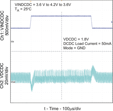 Figure 25. Line Transient Response (DC-DC PFM Mode)
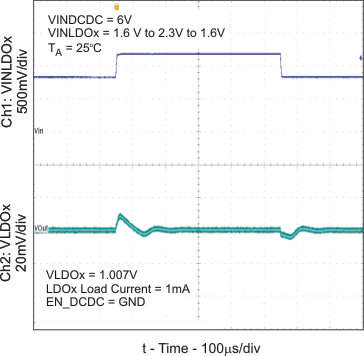 Figure 27. Line Transient Response (LDOx)
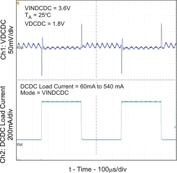 Figure 29. Load Transient Response (DC-DC PWM Mode)
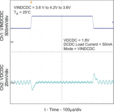 Figure 26. Line Transient Response (DC-DC PWM Mode)
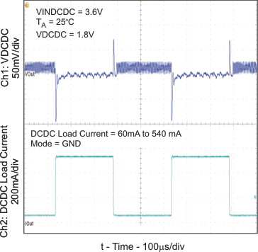 Figure 28. Load Transient Response (DC-DC PFM Mode)
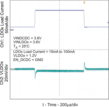 Figure 30. Load Transient Response (LDOx)
10.2.2 Typical TPS65001 Application
10.2.2.1 Design Requirements
For this design example, use the parameters listed in Table 5.
Table 5. Design Parameters
| RESOURCES | VOLTAGE |
|---|---|
| SW | 1.2 V |
| VLDO1 | 1.8 V |
| VLDO2 | 2.8 V |
10.2.3 Typical TPS650001 Application
Table 6. Design Parameters
| RESOURCES | VOLTAGE |
|---|---|
| SW | 1.2 V |
| VLDO1 | 3.3 V |
| VLDO2 | 1.8 V |
10.2.4 Typical TPS650061 Application
10.2.4.1 Design Requirements
For this design example, use the parameters listed in Table 7.
Table 7. Design Parameters
| RESOURCES | VOLTAGE |
|---|---|
| SW | 1.2 V |
| VLDO1 | 3.3 V |
| VLDO2 | 1.8 V |
