SLVS810C June   2009  – September 2015 TPS65000 , TPS650001 , TPS650003 , TPS650006 , TPS65001 , TPS650061

PRODUCTION DATA.  

  1. Features
  2. Applications
  3. Description
  4. Revision History
  5. Description (continued)
  6. Device Options
  7. Pin Configuration and Functions
  8. Specifications
    1. 8.1 Absolute Maximum Ratings
    2. 8.2 ESD Ratings
    3. 8.3 Recommended Operating Conditions
    4. 8.4 Thermal Information
    5. 8.5 Electrical Characteristics
    6. 8.6 Switching Characteristics
    7. 8.7 Dissipation Ratings
    8. 8.8 Typical Characteristics
  9. Detailed Description
    1. 9.1 Overview
    2. 9.2 Functional Block Diagram
    3. 9.3 Feature Description
      1. 9.3.1 Step-Down Converter
      2. 9.3.2 Soft Start
      3. 9.3.3 Linear Regulators
      4. 9.3.4 Oscillator and Spread Spectrum Clock Generation
      5. 9.3.5 Power Good
      6. 9.3.6 Supply Voltage Supervisor (SVS) [TPS65001 and TPS650061 Only]
    4. 9.4 Device Functional Modes
  10. 10Application and Implementation
    1. 10.1 Application Information
    2. 10.2 Typical Application
      1. 10.2.1 Typical TPS65000 Application
        1. 10.2.1.1 Design Requirements
        2. 10.2.1.2 Detailed Design Procedure
          1. 10.2.1.2.1 Output Filter Design (Inductor and Output Capacitor)
            1. 10.2.1.2.1.1 Inductor Selection
            2. 10.2.1.2.1.2 Output Capacitor Selection
            3. 10.2.1.2.1.3 Input Capacitor Selection
        3. 10.2.1.3 Application Curves
      2. 10.2.2 Typical TPS65001 Application
        1. 10.2.2.1 Design Requirements
      3. 10.2.3 Typical TPS650001 Application
      4. 10.2.4 Typical TPS650061 Application
        1. 10.2.4.1 Design Requirements
  11. 11Power Supply Recommendations
  12. 12Layout
    1. 12.1 Layout Guidelines
    2. 12.2 Layout Example
  13. 13Device and Documentation Support
    1. 13.1 Device Support
      1. 13.1.1 Third-Party Products Disclaimer
    2. 13.2 Documentation Support
      1. 13.2.1 Related Documentation
    3. 13.3 Related Links
    4. 13.4 Community Resources
    5. 13.5 Trademarks
    6. 13.6 Electrostatic Discharge Caution
    7. 13.7 Glossary
  14. 14Mechanical, Packaging, and Orderable Information

パッケージ・オプション

メカニカル・データ(パッケージ|ピン)
サーマルパッド・メカニカル・データ
発注情報

12 Layout

12.1 Layout Guidelines

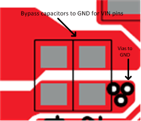
  • The VINDCDC and VINLDOx pins must be bypassed to ground with a low-ESR ceramic bypass capacitor. TI recommends the typical bypass capacitance is 10 μF and 2.2 μF with a X5R dielectric.
  • The optimum placement is closest to the VINDCDCx and VINLDOx pins of the device. Minimize the loop area formed by the bypass capacitor connection, the VINDCDC and VINLDO pins, and the thermal pad of the device.
  • The thermal pad must be tied to the PCB ground plane with multiple vias.
  • The VLDOx and VDCDCx pins (feedback pins) traces must be routed away from any potential noise source to avoid coupling.
  • VODC output capacitance must be placed immediately at the VODC pin. Excessive distance between the capacitance and DCDCx pin may cause poor converter performance.
  • AGND star back to PGND as close to IC as possible.
  • DGND connect to thermal pad.

12.2 Layout Example
TPS65000 TPS65001 TPS650001 TPS650003 TPS650006 TPS650061 Layout_Example_1.gif Figure 34. Layout Recommendation
TPS65000 TPS65001 TPS650001 TPS650003 TPS650006 TPS650061 Layout_Example_2.gif Figure 35. Bypass Capacitor and Via Placement Recommendation