SLVS810C June 2009 – September 2015 TPS65000 , TPS650001 , TPS650003 , TPS650006 , TPS65001 , TPS650061
PRODUCTION DATA.
- 1 Features
- 2 Applications
- 3 Description
- 4 Revision History
- 5 Description (continued)
- 6 Device Options
- 7 Pin Configuration and Functions
- 8 Specifications
- 9 Detailed Description
- 10Application and Implementation
- 11Power Supply Recommendations
- 12Layout
- 13Device and Documentation Support
- 14Mechanical, Packaging, and Orderable Information
パッケージ・オプション
メカニカル・データ(パッケージ|ピン)
- RTE|16
サーマルパッド・メカニカル・データ
- RTE|16
発注情報
8 Specifications
8.1 Absolute Maximum Ratings
over operating free-air temperature range (unless otherwise noted)(1)| MIN | MAX | UNIT | |||
|---|---|---|---|---|---|
| Input voltage range | On all pins except AGND, PGND, EN_DCDC, VLDO1, VLDO2, FB_LDO1, FB_LDO2, FB_DCDC pins with respect to AGND | –0.3 | 7 | V | |
| On EN_DCDC with respect to AGND | –0.3 | VIN + 0.3, ≤ 7 | |||
| Output voltage range | On VLDO1, VLDO2, FB_LDO1, FB_LDO2, FB_DCDC | –0.3 | 3.6 | V | |
| Current | VINDCDC, SW, PGND, | 1800 | mA | ||
| VINLDO1/2, VLDO1/2, AGND | 800 | mA | |||
| At all other pins | 1 | mA | |||
| Continuous total power dissipation | See Dissipation Ratings | ||||
| Operating free-air temperature, TA | –40 | 85 | °C | ||
| Maximum junction temperature, TJ | 125 | °C | |||
| Storage temperature, Tstg | –65 | 150 | °C | ||
(1) Stresses beyond those listed under Absolute Maximum Ratings may cause permanent damage to the device. These are stress ratings only and functional operation of the device at these or any other conditions beyond those indicated under Recommended Operating Conditions is not implied. Exposure to absolute-maximum-rated conditions for extended periods may affect device reliability.
8.2 ESD Ratings
| VALUE | UNIT | |||
|---|---|---|---|---|
| V(ESD) | Electrostatic discharge | Human body model (HBM), per ANSI/ESDA/JEDEC JS-001, all pins(1) | ±2500 | V |
| Charged device model (CDM), per JEDEC specification JESD22-C101, all pins(2) | ±2000 | |||
| Machine model (MM) | ±750 | |||
(1) JEDEC document JEP155 states that 500-V HBM allows safe manufacturing with a standard ESD control process.
(2) JEDEC document JEP157 states that 250-V CDM allows safe manufacturing with a standard ESD control process.
8.3 Recommended Operating Conditions
| MIN | NOM | MAX | UNIT | ||
|---|---|---|---|---|---|
| L1 | SW pin inductor | 1.5 | 2.2 | 3.3 | μH |
| CI | Input capacitor at VINDCDC | 10 | μF | ||
| Input capacitor at VINLDO1/2 | 2.2 | μF | |||
| CO | Output capacitor for DCDC | 10 | 22 | μF | |
| Output capacitor for LDO1/2 | 2.2 | μF | |||
| IO | DC-DC converter output current | 600 | mA | ||
| DC-DC converter output current (TPS650061 ONLY) | 1000 | mA | |||
| LDO1 output current | 300 | mA | |||
| LDO2 output current | 300 | mA | |||
| TA | Operating ambient temperature | –40 | 85 | °C | |
8.4 Thermal Information
| THERMAL METRIC(1) | TPS6500x | UNIT | ||
|---|---|---|---|---|
| RTE (WQFN) | RUK (WQFN) | |||
| 16 PINS | 20 PINS | |||
| RθJA | Junction-to-ambient thermal resistance | 44.7 | 46.2 | °C/W |
| RθJC(top) | Junction-to-case (top) thermal resistance | 41.7 | 51 | °C/W |
| RθJB | Junction-to-board thermal resistance | 16 | 17.8 | °C/W |
| ψJT | Junction-to-top characterization parameter | 0.4 | 0.7 | °C/W |
| ψJB | Junction-to-board characterization parameter | 16 | 17.8 | °C/W |
| RθJC(bot) | Junction-to-case (bottom) thermal resistance | 4.4 | 4.5 | °C/W |
(1) For more information about traditional and new thermal metrics, see the Semiconductor and IC Package Thermal Metrics application report, SPRA953.
8.5 Electrical Characteristics
Over full operating ambient temperature range, typical values are at TA = 25°C. Unless otherwise noted, specifications apply for condition VIN = EN_LDOx = EN_DCDC = 3.6 V. External components L = 2.2 μH, COUT = 10 μF, CIN = 4.7 μF, (see the Typical Application section).| PARAMETER | TEST CONDITIONS | MIN | TYP | MAX | UNIT | |
|---|---|---|---|---|---|---|
| OPERATING VOLTAGE | ||||||
| VIN | Input voltage for VINDCDC of DC-DC converter | 2.3 | 6 | V | ||
| Input voltage for LDO1 (VINLDO1) | See (1) | 1.6 | 6 | |||
| Input voltage for LDO2 (VINLDO2) | See (1) | 1.6 | 6 | |||
| UVLO | Internal undervoltage lockout threshold | VCC falling | 1.72 | 1.77 | 1.82 | V |
| Internal undervoltage lockout hysteresis | 160 | mV | ||||
| SUPPLY CURRENT TPS65000 | ||||||
| IQ | Operating quiescent current | MODE low, EN_DCDC high, EN_LDO1/2 low, IOUT = 0 mA and no switching |
23 | 32 | μA | |
| MODE low, EN_DCDC low, EN_LDO1/2 high, IOUT = 0 mA IOUT = 0 mA and no switching(2) |
50 | 57 | ||||
| EN_DCDC high, MODE high, EN_LDO1/2 low, IOUT = 0 mA |
4 | mA | ||||
| ISD | Shutdown Current | EN_DCDC low EN_LDO1 and EN_LDO2 low | 0.16 | 2.2 | μA | |
| SUPPLY CURRENT TPS65001 | ||||||
| IQ | Operating quiescent current | MODE low, EN_DCDC high, EN_LDO1/2 low, IOUT = 0 mA and no switching |
24 | 37 | μA | |
| MODE low, EN_DCDC low, EN_LDO1/2 high, IOUT = 0 mA IOUT = 0 mA and no switching(2) |
55 | 62 | μA | |||
| EN_DCDC high, MODE high, EN_LDO1/2 low, IOUT = 0 mA |
4 | mA | ||||
| ISD | Shutdown Current | EN_DCDC low EN_LDO1 and EN_LDO2 low | 11 | 17 | μA | |
| DIGITAL PINS (EN_DCDC, EN_LDO1, EN_LDO2, MODE, PG, MR, RST) | ||||||
| VIH | High-level input voltage | 1.2 | V | |||
| VIL | Low-level input voltage | 0.4 | V | |||
| VOL | Low-level output voltage | PG and RST pins only, IO = -100 μA | 0.4 | V | ||
| Ilkg | Input leakage current | MODE, EN_DCDC, EN_LDO1, EN_LDO2 tied to GND or VINDCDC | 0.01 | 0.1 | μA | |
| OSCILLATOR | ||||||
| fSW | Oscillator frequency | 1.722 | 2.25 | 2.847 | MHz | |
| STEP DOWN CONVERTER POWER SWITCH | ||||||
| RDS(on) | High-side MOSFET ON-resistance | VINDCDC = VGS = 3.6 V | 240 | 480 | mΩ | |
| Low-side MOSFET ON-resistance | 185 | 380 | ||||
| IO | DC-output current | 2.3 V ≤ VINDCDC ≤ 2.5 V | 300 | mA | ||
| 2.5 V ≤ VINDCDC ≤ 6 V | 600 | |||||
| IO | DC-output current (TPS650061 ONLY) | 2.7 V ≤ VINDCDC ≤ 6 V | 1000 | mA | ||
| ILIMF | Forward current limit PMOS and NMOS | 2.3 V ≤ VINDCDC ≤ 6 V | 800 | 1000 | 1400 | mA |
| ILIMF | Forward current limit PMOS and NMOS (TPS650061 ONLY) | 2.7 V ≤ VINDCDC ≤ 6 V | 1200 | 1500 | 1680 | mA |
| TSD | Thermal shutdown | Increasing junction temperature | 150 | °C | ||
| Thermal shutdown hysteresis | Decreasing junction temperature | 30 | ||||
| STEP DOWN CONVERTER OUTPUT VOLTAGE | ||||||
| VDCDC | Adjustable output voltage range, DCDC | 0.6 | VINDCDC | V | ||
| FB_DCDC pin current | 0.1 | μA | ||||
| Vref | Internal reference voltage | 0.594 | 0.6 | 0.606 | V | |
| VDCDC | Output Voltage Accuracy (PWM Mode)(3) | MODE = high, 2.3 ≤ VINDCDC ≤ 6 V |
–1.5% | 0% | 1.5% | |
| Output Voltage Accuracy (PFM mode) (4) | MODE low 1% voltage positioning active |
1% | ||||
| Load regulation (PWM mode) | MODE high | 0.5% | A | |||
| RDIS | Internal discharge resistance at SW | EN_DCDC low | 450 | Ω | ||
| LOW DROP OUT REGULATORS | ||||||
| VI | Input voltage for LDOx (VINLDOx) | 1.6 | 6 | V | ||
| VO | Adjustable output voltage, LDOx (VLDOx)(5) | 0.73 | VINLDOx – VDO | V | ||
| IO | Continuous Pass FET Current | 300 | mA | |||
| ISC | Short circuit current limit | 2.3 V ≤ VINLDOx | 340 | 700 | mA | |
| VINLDOx < 2.3V | 210 | 700 | ||||
| FB_LDOx pin current | 0.1 | μA | ||||
| FB_LDOx voltage | Adjustable VOUT mode only | 0.5 | V | |||
| VDO | Dropout Voltage (6) | VINLDOx ≥ 2.3 V, IOUT = 250 mA | 370 | mV | ||
| VINLDOx < 2.3V IOUT = 175 mA | 370 | mV | ||||
| LOW DROP OUT REGULATORS (continued) | ||||||
| Output Voltage Accuracy (7) | IO = 1 mA to 300 mA, VINLDOx = 2.3 V – 6 V, VLDOx = 1.2 V |
–3.5% | 3.5% | |||
| IO = 1mA to 175 mA VINLDOx = 1.6 V – 6 V, VLDOx = 1.2 V |
–3.5% | 3.5% | ||||
| Load regulation | IO = 1mA to 300 mA VINLDOx = 3.6 V VLDOx = 1.2 V |
–1.5% | 1.5% | |||
| Line regulation | VINLDOx = 1.6 V – 6 V VLDOx = 1.2 V at IO = 1 mA |
–0.5% | 0.5% | |||
| PSRR | Power Supply Rejection Ratio | fNOISE ≤ 10 kHz, COUT ≥ 2.2 μF, VIN = 2.3 V, VOUT = 1.3 V IOUT = 10 mA |
40 | dB | ||
| RDIS | Internal discharge resistance at VLDOx | EN_LDOx low | 450 | Ω | ||
| TSD | Thermal shutdown | Increasing temperature | 150 | °C | ||
| Thermal shutdown hysteresis | Decreasing temperature | 30 | °C | |||
| SUPPLY VOLTAGE SUPERVISOR | ||||||
| VIN | Input voltage for RSTSNS pin | 0 | 6 | V | ||
| t MRDEGLITCH | MR Deglitch time | 1 | ms | |||
| VIH | Input high voltage | MR pin only | 1.2 | 6 | V | |
| VIL | Input low voltage | MR pin only | 0 | 0.4 | V | |
| Ilkg | High-input leakage current | RST pin | 0.01 | 0.1 | μA | |
| VOL | Output low voltage | RST pin only, IO = –100 μA | 0.4 | V | ||
| ITRST | Reset timer capacitor current | 1.6 | 2 | 2.2 | μA | |
| Reset voltage trip voltage | Voltage rising (Reset time begins) | 0.58 | 0.6 | 0.63 | V | |
| Reset voltage trip hysteresis | Voltage falling (RST pulled low) | –5% | ||||
(1) The design principle lets only VINDCDC be the highest supply in the system if different voltage input supplies separately to DC-DC converter and LDOs, meaning VINDCDC ≥ VINLDO1, VINDCDC ≥ VINLDO2.
(2) The max quiescent current of enabling LDOs is 8 μA higher for TPS650001, TPS650003, TPS650006, and TPS650061.
(3) For VINDCDC = VDCDC + 1 V
(4) In PFM Mode, the internal reference voltage is typ 1.01 × VREF.
(5) Maximum output voltage VLDOx = 3.6 V.
(6) VDO = VINLDOx – VLDOx where VINLDOx = VLDOx (nominal) – 100 mV
(7) Output voltage specification does not include tolerance of external programming resistors.
8.6 Switching Characteristics
over operating free-air temperature range (unless otherwise noted)| PARAMETER | TEST CONDITIONS | MIN | TYP | MAX | UNIT | |
|---|---|---|---|---|---|---|
| STEP DOWN CONVERTER OUTPUT VOLTAGE | ||||||
| tStart | Start-up time | EN_DCDC to start of switching (10%) | 250 | μs | ||
| tRamp | VDCDC ramp-up time | VDCDC ramp from 10% to 90% | 250 | μs | ||
| LOW DROP OUT REGULATORS | ||||||
| tRAMP | VLDOx Ramp Time | VLDOx ramp from 10% to 90% | 200 | μs | ||
8.7 Dissipation Ratings
| DEVICE | PACKAGE | RθJA | RθJB | TA ≤ 25°C POWER RATING |
TA = 70°C POWER RATING |
TA = 85°C POWER RATING |
|---|---|---|---|---|---|---|
| TPS65000/01(1) | RTE/RUK | 270°C/W | 14°C/W | 370 mW | 204 mW | 148 mW |
| TPS65000/01(2) | 48.7°C/W | 14°C/W | 2.05 W | 1.13 W | 821 mW |
(1) The JEDEC low-K (1s) board used to derive this data was a 3 in × 3 in, two-layer board with 2-oz copper traces on top of the board.
(2) The JEDEC high-K (2s2p) board used to derive this data was a 3 in × 3 in, multilayer board with 1-oz internal power and ground.
8.8 Typical Characteristics
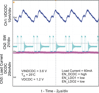 Figure 5. Output Voltage Ripple (DC-DC PFM Mode)
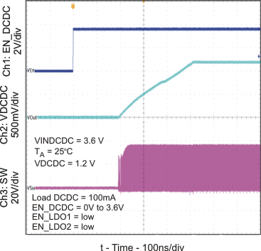 Figure 7. Startup Timing (DC-DC)
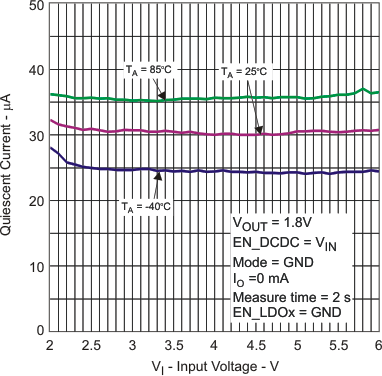 Figure 9. TPS650001 Quiescent Current (DC-DC PFM Mode) vs Input Voltage
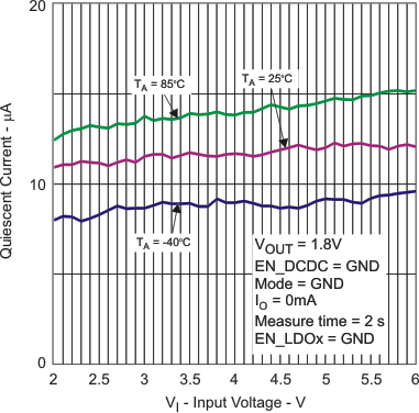 Figure 11. TPS650001 Shutdown Current vs Input Voltage
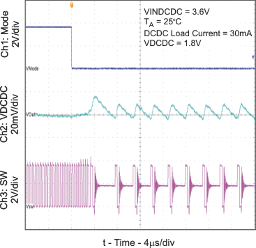 Figure 13. PWM to PFM Transition (DC-DC)
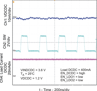 Figure 6. Output Voltage Ripple (DC-DC PWM Mode)
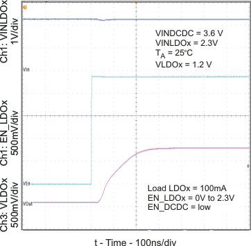 Figure 8. Start-Up Timing (LDOx)
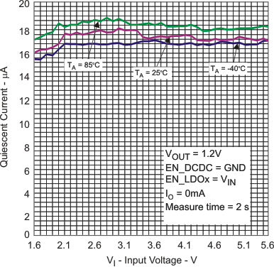 Figure 10. TPS650001 Quiescent Current (LDOx) vs Input Voltage
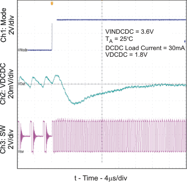 Figure 12. PFM to PWM Transition (DC-DC)
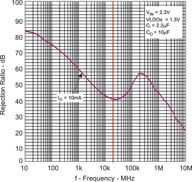 Figure 14. Power Supply Rejection Ratio (LDOx) vs Frequency
