SWCS046U March 2010 – October 2014 TPS65910
PRODUCTION DATA.
- 1Device Overview
- 2Revision History
- 3 Device Comparison
- 4Terminal Configuration and Functions
-
5Specifications
- 5.1 Absolute Maximum Ratings
- 5.2 Handling Ratings
- 5.3 Recommended Operating Conditions
- 5.4 Thermal Resistance Characteristics for RSL Package
- 5.5 I/O Pullup and Pulldown Characteristics
- 5.6 Digital I/O Voltage Electrical Characteristics
- 5.7 I2C Interface and Control Signals
- 5.8 Power Consumption
- 5.9 Power References and Thresholds
- 5.10 Thermal Monitoring and Shutdown
- 5.11 32-kHz RTC Clock
- 5.12 Backup Battery Charger
- 5.13 VRTC LDO
- 5.14 VIO SMPS
- 5.15 VDD1 SMPS
- 5.16 VDD2 SMPS
- 5.17 VDD3 SMPS
- 5.18 VDIG1 and VDIG2 LDO
- 5.19 VAUX33 and VMMC LDO
- 5.20 VAUX1 and VAUX2 LDO
- 5.21 VDAC and VPLL LDO
- 5.22
Timing and Switching Characteristics
- 5.22.1 Switch-On/-Off Sequences and Timing
- 5.22.2
Power Control Timing
- 5.22.2.1 Device Turn-On/Off With Rising/Falling Input Voltage
- 5.22.2.2 Device State Control Through PWRON Signal
- 5.22.2.3 Device SLEEP State Control
- 5.22.2.4 Power Supplies State Control Through the SCLSR_EN1 and SDASR_EN2 Signals
- 5.22.2.5 VDD1 and VDD2 Voltage Control Through SCLSR_EN1 and SDASR_EN2 Signals
- 5.22.2.6 SMPS Switching Synchronization
-
6Detailed Description
- 6.1 Power Reference
- 6.2 Power Sources
- 6.3 Embedded Power Controller
- 6.4 32-kHz RTC Clock
- 6.5 RTC
- 6.6 Backup Battery Management
- 6.7 Backup Registers
- 6.8 I2C Interface
- 6.9 Thermal Monitoring and Shutdown
- 6.10 Interrupts
- 6.11 Package Description
- 6.12 Functional Registers
- 7Device and Documentation Support
- 8Mechanical Packaging and Orderable Information
パッケージ・オプション
メカニカル・データ(パッケージ|ピン)
- RSL|48
サーマルパッド・メカニカル・データ
- RSL|48
発注情報
5 Specifications
5.1 Absolute Maximum Ratings(1)(2)
over operating free-air temperature range (unless otherwise noted)| MIN | MAX | UNIT | ||
|---|---|---|---|---|
| Voltage range on pins/balls VCC1, VCC2, VCCIO, VCC3, VCC4, VCC5, VCC6, VCC7 | –0.3 | 7 | V | |
| Voltage range on pins/balls VDDIO | –0.3 | 3.6 | V | |
| Voltage range on pins/balls OSC32KIN, OSC32KOUT, BOOT1, BOOT0 | –0.3 | VRTCMAX + 0.3 | V | |
| Voltage range on pins/balls SDA_SDI, SCL_SCK, SDASR_EN2, SCLSR_EN1, SLEEP, INT1, CLK32KOUT, NRESPWRON | –0.3 | VDDIOMAX + 0.3 | V | |
| Voltage range on pins/balls PWRON | –0.3 | 7 | V | |
| Voltage range on pins/balls PWRHOLD(3) GPIO_CKSYNC(4) | –0.3 | 7 | V | |
| Peak output current on all other terminals than power resources | –5 | 5 | mA | |
5.2 Handling Ratings
| MIN | MAX | UNIT | ||||
|---|---|---|---|---|---|---|
| Tstg | Storage temperature range | –45 | 150 | °C | ||
| VESD | Electrostatic discharge (ESD) performance: | Human Body Model (HBM), per ANSI/ESDA/JEDEC JS001(1) | –2 | 2 | kV | |
| Charged Device Model (CDM), per JESD22-C101(2) |
All pins | –500 | 500 | V | ||
5.3 Recommended Operating Conditions
over operating free-air temperature range (unless otherwise noted)Note 1: VCC7 should be connected to the highest supply that is connected to the device VCCx pin. The exception is that VCC2 and VCC4 can be higher than VCC7.
Note 2: VCC2 and VCC4 must be connected together (to the same voltage).
Note 3: If VDD3 boost is used, VAUX33 must be set to 2.8 V or higher and enabled before VDD3.
| PARAMETER | TEST CONDITIONS | MIN | NOM | MAX | UNIT | |
|---|---|---|---|---|---|---|
| VCC: Input voltage range on pins/balls VCC1, VCC2, VCCIO, VCC3, VCC4, VCC5, VCC7 | 2.7 | 3.6 | 5.5 | V | ||
| VCCP: Input voltage range on pins/balls VCC6 | 1.7 | 3.6 | 5.5 | V | ||
| Input voltage range on pins/balls VDDIO | 1.65 | 1.8/3.3 | 3.45 | V | ||
| Input voltage range on pins/balls PWRON | 0 | 3.6 | 5.5 | V | ||
| Input voltage range on pins/balls SDA_SDI, SCL_SCK, SDASR_EN2, SCLSR_EN1, SLEEP | 1.65 | VDDIO | 3.45 | V | ||
| Input voltage range on pins/balls PWRHOLD, GPIO_CKSYNC | 1.65 | VDDIO | 5.5 | V | ||
| Input voltage range on balls BOOT1, BOOT0, OSC32KIN | 1.65 | VRTC | 1.95 | V | ||
| Operating free-air temperature, TA | –40 | 27 | 85 | °C | ||
| Junction temperature, TJ | –40 | 27 | 125 | °C | ||
| Storage temperature range | –65 | 27 | 150 | °C | ||
| Lead temperature (soldering, 10 s) | 260 | °C | ||||
| Power References | ||||||
| VREF filtering capacitor CO(VREF) | Connected from VREF to REFGND | 100 | nF | |||
| VDD1 SMPS | ||||||
| Input capacitor CI(VCC1) | X5R or X7R dielectric | 10 | µF | |||
| Filter capacitor CO(VDD1) | X5R or X7R dielectric | 4 | 10 | 12 | µF | |
| CO filter capacitor ESR | f = 3 MHz | 10 | 300 | mΩ | ||
| Inductor LO(VDD1) | 2.2 | µH | ||||
| LO inductor dc resistor DCRL | 125 | mΩ | ||||
| VDD2 SMPS | ||||||
| Input capacitor CI(VCC2) | X5R or X7R dielectric | 10 | µF | |||
| Filter capacitor CO(VDD2) | X5R or X7R dielectric | 4 | 10 | 12 | µF | |
| CO filter capacitor ESR | f = 3 MHz | 10 | 300 | mΩ | ||
| Inductor LO(VDD2) | 2.2 | µH | ||||
| LO inductor dc resistor DCRL | 125 | mΩ | ||||
| VIO SMPS | ||||||
| Input capacitor CI(VIO) | X5R or X7R dielectric | 10 | µF | |||
| Filter capacitor CO(VIO) | X5R or X7R dielectric | 4 | 10 | 12 | µF | |
| CO filter capacitor ESR | f = 3 MHz | 10 | 300 | mΩ | ||
| Inductor LO(VIO) | 2.2 | µH | ||||
| LO inductor dc resistor DCRL | 125 | mΩ | ||||
| VDIG1 LDO | ||||||
| Input capacitor CI(VCC6) | X5R or X7R dielectric | 4.7 | µF | |||
| Filtering capacitor CO(VDIG1) | 0.8 | 2.2 | 2.64 | µF | ||
| CO filtering capacitor ESR | 0 | 500 | mΩ | |||
| VDIG2 LDO | ||||||
| Filtering capacitor CO(VDIG2) | 0.8 | 2.2 | 2.64 | µF | ||
| CO filtering capacitor ESR | 0 | 500 | mΩ | |||
| VPLL LDO | ||||||
| Input capacitor CI(VCC5) | X5R or X7R dielectric | 4.7 | µF | |||
| Filtering capacitor CO(VPLL) | 0.8 | 2.2 | 2.64 | µF | ||
| CO filtering capacitor ESR | 0 | 500 | mΩ | |||
| VDAC LDO | ||||||
| Filtering capacitor CO(VDAC) | 0.8 | 2.2 | 2.64 | µF | ||
| CO filtering capacitor ESR | 0 | 500 | mΩ | |||
| VMMC LDO | ||||||
| Input capacitor CI(VCC4) | X5R or X7R dielectric | 4.7 | µF | |||
| Filtering capacitor CO(VMMC) | 0.8 | 2.2 | 2.64 | µF | ||
| CO filtering capacitor ESR | 0 | 500 | mΩ | |||
| VAUX33 LDO | ||||||
| Filtering capacitor CO(VAUX33) | 0.8 | 2.2 | 2.64 | µF | ||
| CO filtering capacitor ESR | 0 | 500 | mΩ | |||
| VAUX1 LDO | ||||||
| Input capacitor CI(VCC3) | X5R or X7R dielectric | 4.7 | µF | |||
| Filtering capacitor CO(VAUX1) | 0.8 | 2.2 | 2.64 | µF | ||
| CO filtering capacitor ESR | 0 | 500 | mΩ | |||
| VAUX2 LDO | ||||||
| Filtering capacitor CO(VAUX2) | 0.8 | 2.2 | 2.64 | µF | ||
| CO filtering capacitor ESR | 0 | 500 | mΩ | |||
| VRTC LDO | ||||||
| Input capacitor CI(VCC7) | X5R or X7R dielectric | 4.7 | µF | |||
| Filtering capacitor CO(VRTC) | 0.8 | 2.2 | 2.64 | µF | ||
| CO filtering capacitor ESR | 0 | 500 | mΩ | |||
| VDD3 SMPS | ||||||
| Input capacitor CI(VDD3) | X5R or X7R dielectric | 4.7 | µF | |||
| Filter capacitor CO(VDD3) | X5R or X7R dielectric | 4 | 10 | 12 | µF | |
| CO filter capacitor ESR | f = 1 MHz | 10 | 300 | mΩ | ||
| Inductor LO(VDD3) | 2.8 | 4.7 | 6.6 | µH | ||
| LO inductor DC resistor DCRL | 50 | 500 | mΩ | |||
| Backup Battery | ||||||
| Backup battery capacitor CBB | Battery or superCap supplying VBACKUP | 5 | 10 | 2000 | mF | |
| Capacitor supplying VBACKUP | 1 | 40 | µF | |||
| Series resistors | 5 to 15 mF | 10 | 1500 | Ω | ||
| 100 to 2000 mF | 5 | 15 | ||||
| I2C Interfaces | ||||||
| SDA_SDI, SCL_SCK, SDASR_EN2, SCLSR_EN1 external pull-up resistor | Connected to VDDIO | 1.2 | kΩ | |||
| Crystal Oscillator (connected from OSC32KIN to OSC32KOUT) | ||||||
| Crystal frequency | at specified load cap value | 32.768 | kHz | |||
| Crystal tolerance | at 27°C | –20 | 0 | 20 | ppm | |
| Frequency Temperature coefficient. | Oscillator contribution (not including crystal variation) | –0.5 | 0.5 | ppm/°C | ||
| Secondary temperature coefficient | –0.04 | –0.035 | –0.03 | ppm/°C2 | ||
| Voltage coefficient | –2 | 2 | ppm/V | |||
| Max crystal series resistor | at fundamental frequency | 90 | kΩ | |||
| Crystal load capacitor | According to crystal data sheet | 6 | 12.5 | pF | ||
| Load crystal oscillator Coscin, Coscout | parallel mode including parasitic PCB capacitor | 12 | 25 | pF | ||
| Quality factor | 8000 | 80000 | ||||
5.4 Thermal Resistance Characteristics for RSL Package
| NAME | DESCRIPTION | °C/W(1)(2) | AIR FLOW (m/s)(3) |
|---|---|---|---|
| RΘJC | Junction-to-case (top) | 16.4 | 0.00 |
| RΘJB | Junction-to-board | 5.6 | 0.00 |
| RΘJA
(High k PCB) |
Junction-to-free air | 37 | 0.00 |
| PsiJT | Junction-to-package top | 0.2 | 0.00 |
| PsiJB | Junction-to-board | 5.6 | 0.00 |
| RΘJC | Junction-to-case (bottom) | 1.3 | 0.00 |
- JESD51-2, Integrated Circuits Thermal Test Method Environmental Conditions - Natural Convection (Still Air)
- JESD51-3, Low Effective Thermal Conductivity Test Board for Leaded Surface Mount Packages
- JESD51-7, High Effective Thermal Conductivity Test Board for Leaded Surface Mount Packages
- JESD51-9, Test Boards for Area Array Surface Mount Package Thermal Measurements
5.5 I/O Pullup and Pulldown Characteristics(1)
over operating free-air temperature range (unless otherwise noted)| PARAMETER | TEST CONDITIONS | MIN | TYP | MAX | UNIT | |
|---|---|---|---|---|---|---|
| SDA_SDI, SCL_SCK, SDASR_EN2, SCLSR_EN1 Programmable pullup (DFT, default inactive) | Grounded, VDDIO = 1.8 V | –45% | 8 | +45% | kΩ | |
| SLEEP programmable pulldown (default active) | at 1.8 V, VRTC = 1.8 V | 2 | 4.5 | 10 | µA | |
| PWRHOLD programmable pulldown (default active) | at 1.8 V, VRTC = 1.8 V, VCC7 = 2.7 V | 2 | 4.5 | 10 | µA | |
| at 5.5 V, VRTC = 1.8 V, VCC7 = 5.5 V | 7 | 14 | 30 | |||
| BOOT0, BOOT1 programmable pulldown (default active) | at 1.8 V, VRTC = 1.8 V | 2 | 4.5 | 10 | µA | |
| NRESPWRON pulldown | at 1.8 V, VCC7 = 5.5 V, OFF state | 2 | 4.5 | 10 | µA | |
| 32KCLKOUT pulldown (disabled in active-sleep state) | at 1.8 V, VRTC = 1.8 V, OFF state | 2 | 4.5 | 10 | µA | |
| PWRON programmable pullup (default active) | Grounded, VCC7 = 5.5 V | –40 | –31 | –15 | µA | |
| GPIO_CKSYNC programmable pullup (default active) | Grounded, VRTC = 1.8 V | –27 | –18 | –9 | µA | |
5.6 Digital I/O Voltage Electrical Characteristics
over operating free-air temperature range (unless otherwise noted)| PARAMETER | MIN | TYP | MAX | UNIT | ||
|---|---|---|---|---|---|---|
| Related I/O: PWRON | ||||||
| Low-level input voltage, VIL | 0.3 x VCC7 | V | ||||
| High-level input voltage, VIH | 0.7 x VCC7 | V | ||||
| Related I/Os: PWRHOLD, GPIO_CKSYNC | ||||||
| Low-level input voltage, VIL | 0.45 | V | ||||
| High-level input voltage, VIH | 1.3 | VDDIO/VCC7 | VCC7 | V | ||
| Related I/Os: BOOT0, BOOT1, OSC32KIN | ||||||
| Low-level input voltage, VIL | 0.35 x VRTC | V | ||||
| High-level input voltage, VIH | 0.65 x VRTC | V | ||||
| Related I/Os: SLEEP | ||||||
| Low-level input voltage, VIL | 0.35 x VDDIO | V | ||||
| High-level input voltage, VIH | 0.65 x VDDIO | V | ||||
| Related I/Os: NRESPWRON, INT1, 32KCLKOUT | ||||||
| Low-level output voltage, VOL | IOL = 100 µA | 0.2 | V | |||
| IOL = 2 mA | 0.45 | V | ||||
| High-level output voltage, VOH | IOH = 100 µA | VDDIO – 0.2 | V | |||
| IOH = 2 mA | VDDIO – 0.45 | V | ||||
| Related Open-Drain I/Os: GPIO0 | ||||||
| Low-level output voltage, VOL | IOL = 100 µA | 0.2 | V | |||
| IOL = 2 mA | 0.45 | V | ||||
| I2C-Specific Related I/Os: SCL, SDA, SCLSR_EN1, SDASR_EN2 | ||||||
| Low-level input voltage, VIL | –0.5 | 0.3 x VDDIO | V | |||
| High-level input voltage, VIH | 0.7 x VDDIO | V | ||||
| Hysteresis | 0.1 x VDDIO | V | ||||
| Low-level output voltage, VOL at 3 mA (sink current), VDDIO = 1.8 V | 0.2 × VDDIO | V | ||||
| Low-level output voltage, VOL at 3 mA (sink current), VDDIO = 3.3 V | 0.4 x VDDIO | V | ||||
5.7 I2C Interface and Control Signals
over operating free-air temperature range (unless otherwise noted)| NO. | PARAMETER | TEST CONDITIONS | MIN | TYP | MAX |
|---|---|---|---|---|---|
| INT1 rise and fall times, CL = 5 to 35 pF | 5 | 10 | ns | ||
| NRESPWRON rise and fall times, CL = 5 to 35 pF | 5 | 10 | ns | ||
| SLAVE HIGH–SPEED MODE | |||||
| SCL/SCLSR_EN1 and SDA/SDASR_EN2 rise and fall time, CL = 10 to 100 pF | 10 | 80 | ns | ||
| Data rate | 3.4 | Mbps | |||
| I3 | tsu(SDA-SCLH) | Setup time, SDA valid to SCL high | 10 | ns | |
| I4 | th(SCLL-SDA) | Hold time, SDA valid from SCL low | 0 | 70 | ns |
| I7 | tsu(SCLH-SDAL) | Setup time, SCL high to SDA low | 160 | ns | |
| I8 | th(SDAL-SCLL) | Hold time, SCL low from SDA low | 160 | ns | |
| I9 | tsu(SDAH-SCLH) | Setup time, SDA high to SCL high | 160 | ns | |
| SLAVE FAST MODE | |||||
| SCL/SCLSR_EN1 and SDA/SDASR_EN2 rise and fall time, CL = 10 to 400 pF | 20 + 0.1 × CL |
250 | ns | ||
| Data rate | 400 | Kbps | |||
| I3 | tsu(SDA-SCLH) | Setup time, SDA valid to SCL high | 100 | ns | |
| I4 | th(SCLL-SDA) | Hold time, SDA valid from SCL low | 0 | 0.9 | µs |
| I7 | tsu(SCLH-SDAL) | Setup time, SCL high to SDA low | 0.6 | µs | |
| I8 | th(SDAL-SCLL) | Hold time, SCL low from SDA low | 0.6 | µs | |
| I9 | tsu(SDAH-SCLH) | Setup time, SDA high to SCL high | 0.6 | µs | |
| SLAVE STANDARD MODE | |||||
| SCL/SCLSR_EN1 and SDA/SDASR_EN2 rise and fall time, CL = 10 to 400 pF | 250 | ns | |||
| Data rate | 100 | Kbps | |||
| I3 | tsu(SDA-SCLH) | Setup time, SDA valid to SCL high | ns | ||
| I4 | th(SCLL-SDA) | Hold time, SDA valid from SCL low | 0 | µs | |
| I7 | tsu(SCLH-SDAL) | Setup time, SCL high to SDA low | 4.7 | µs | |
| I8 | th(SDAL-SCLL) | Hold time, SCL low from SDA low | 4 | µs | |
| I9 | tsu(SDAH-SCLH) | Setup time, SDA high to SCL high | 4 | µs | |
| SWITCHING CHARACTERISTICS | |||||
| SLAVE HIGH–SPEED MODE | |||||
| I1 | tw(SCLL) | Pulse duration, SCL low | 160 | ns | |
| I2 | tw(SCLH) | Pulse duration, SCL high | 60 | ns | |
| SLAVE FAST MODE | |||||
| I1 | tw(SCLL) | Pulse duration, SCL low | 1.3 | µs | |
| I2 | tw(SCLH) | Pulse duration, SCL high | 0.6 | µs | |
| SLAVE STANDARD MODE | |||||
| I1 | tw(SCLL) | Pulse duration, SCL low | 4.7 | µs | |
| I2 | tw(SCLH) | Pulse duration, SCL high | 4 | µs | |
5.8 Power Consumption
over operating free-air temperature range (unless otherwise noted)All current consumption measurements are relative to the FULL chip, all VCC inputs set to VBAT voltage.
| PARAMETER | TEST CONDITIONS | MIN | TYP | MAX | UNIT | |
|---|---|---|---|---|---|---|
| Device BACKUP state | VBAT = 2.4 V, VBACKUP = 0 V, | 11 | 16 | µA | ||
| VBAT = 0 V, VBACKUP = 3.2 V | 6 | 9 | ||||
| Device OFF state | VBAT = 3.6 V, CK32K clock running | µA | ||||
| BOOT[1:0] = 00: 32-kHz RC oscillator | 16.5 | 23 | ||||
| BOOT[1:0] = 01: 32-kHz quartz or bypass oscillator, BOOT0P = 0 | 15 | 20 | ||||
| BOOT[1:0] = 01, Backup Battery Charger on, VBACKUP = 3.2 V | 32 | 42 | ||||
| VBAT = 5 V, CK32K clock running: | 20 | 28 | ||||
| BOOT[1:0] = 00: RC oscillator | ||||||
| Device SLEEP state | VBAT = 3.6 V, CK32K clock running, PWRHOLDP = 0 | µA | ||||
| BOOT[1:0] = 00, 3 DC-DCs on, 5 LDOs and VRTC on, no load | 295 | |||||
| BOOT[1:0] = 01, 3 DC-DCs on, 3 LDOs and VRTC on, no load, BOOT0P = 0 | 279 | |||||
| Device ACTIVE state | VBAT = 3.6 V, CK32K clock running, PWRHOLDP = 0 | mA | ||||
| BOOT[1:0] = 00, 3 DC-DCs on, 5 LDOs and VRTC on, no load | 1 | |||||
| BOOT[1:0] = 01, 3 DC-DCs on, 3 LDOs and VRTC on, no load, BOOT0P = 0 | 0.9 | |||||
| BOOT[1:0] = 00, 3 DC-DCs on PWM mode (VDD1_PSKIP = VDD2_PSKIP = VIO_PSKIP = 0), 5 LDOs and VRTC on, no load | 21 | |||||
5.9 Power References and Thresholds
over operating free-air temperature range (unless otherwise noted)| PARAMETER | TEST CONDITIONS | MIN | TYP | MAX | UNIT | |
|---|---|---|---|---|---|---|
| Output reference voltage (VREF terminal) | Device in active or low-power mode | –1% | 0.85 | +1% | V | |
| Main battery charged threshold VMBCH (programmable) |
Measured on VCC7 terminal Triggering monitored through NRESPRWON |
|||||
| VMBCH_VSEL = 11, BOOT[1:0] = 11 or 00 | 3 | V | ||||
| VMBCH_VSEL = 10 | 2.9 | |||||
| VMBCH_VSEL = 01 | 2.8 | |||||
| VMBCH_VSEL = 00 | bypassed | |||||
| Main battery discharged threshold VMBDCH (programmable) |
Measured on VCC7 terminal (MTL prg) Triggering monitored through INT1 |
VMBCH – 100 mV | V | |||
| Main battery low threshold VMBLO (MB comparator) |
Measured on VCC7 terminal (Triggering monitored on terminal NRESPWRON) | 2.5 | 2.6 | 2.7 | V | |
| Main battery high threshold VMBHI | VBACKUP = 0 V, measured on terminal VCC7 (MB comparator) |
2.6 | 2.75 | 3 | V | |
| VBACKUP = 3.2 V, measured on terminal VCC7 | 2.5 | 2.55 | 3 | |||
| Main battery not present threshold VBNPR | Measured on terminal VCC7 (Triggering monitored on terminal VRTC) |
1.9 | 2.1 | 2.2 | V | |
| Ground current (analog references + comparators + backup battery switch) | VCC = 3.6 V | |||||
| Device in OFF state | 8 | µA | ||||
| Device in ACTIVE or SLEEP state | 20 | |||||
5.10 Thermal Monitoring and Shutdown
over operating free-air temperature range (unless otherwise noted)| PARAMETER | TEST CONDITIONS | MIN | TYP | MAX | UNIT | |
|---|---|---|---|---|---|---|
| Hot-die temperature rising threshold | THERM_HDSEL[1:0] = 00 | 117 | °C | |||
| THERM_HDSEL[1:0] = 01 | 121 | |||||
| THERM_HDSEL[1:0] = 10 | 113 | 125 | 136 | |||
| THERM_HDSEL[1:0] = 11 | 130 | |||||
| Hot-die temperature hysteresis | 10 | °C | ||||
| Thermal shutdown temperature rising threshold | 136 | 148 | 160 | °C | ||
| Thermal shutdown temperature hysteresis | 10 | °C | ||||
| Ground current | Device in ACTIVE state, Temp = 27°C, VCC7 = 3.6 V | 6 | µA | |||
5.11 32-kHz RTC Clock
over operating free-air temperature range (unless otherwise noted)| PARAMETER | TEST CONDITIONS | MIN | TYP | MAX | UNIT | |
|---|---|---|---|---|---|---|
| CLK32KOUT rise and fall time | CL = 35 pF | 10 | ns | |||
| Bypass Clock (OSC32KIN: input, OSC32KOUT floating) | ||||||
| Input bypass clock frequency | OSCKIN input | 32 | kHz | |||
| Input bypass clock duty cycle | OSCKIN input | 40% | 60% | |||
| Input bypass clock rise and fall time | 10% – 90%, OSC32KIN input | 10 | 20 | ns | ||
| CLK32KOUT duty cycle | Logic output signal | 40% | 60% | |||
| Bypass clock setup time | 32KCLKOUT output | 1 | ms | |||
| Ground current | Bypass mode | 1.5 | µA | |||
| Crystal oscillator (connected from OSC32KIN to OSC32KOUT) | ||||||
| Output frequency | CK32KOUT output | 32.768 | kHz | |||
| Oscillator startup time | On power on | 2 | s | |||
| Ground current | 1.5 | µA | ||||
| RC oscillator (OSC32KIN: grounded, OSC32KOUT floating) | ||||||
| Output frequency | CK32KOUT output | 32 | kHz | |||
| Output frequency accuracy | at 25°C | –15% | 0% | +15% | ||
| Cycle jitter (RMS) | Oscillator contribution | +10% | ||||
| Output duty cycle | +40% | +50% | +60% | |||
| Settling time | 150 | µs | ||||
| Ground current | Active at fundamental frequency | 4 | µA | |||
5.12 Backup Battery Charger
over operating free-air temperature range (unless otherwise noted)| PARAMETER | TEST CONDITIONS | MIN | TYP | MAX | UNIT | |
|---|---|---|---|---|---|---|
| Backup battery charging current | VBACKUP = 0 to 2.4 V, BBCHEN = 1 | 350 | 500 | 700 | µA | |
| End-of-charge backup battery voltage(1) | VCC7 = 3.6 V, BBSEL = 10 | –3% | 3.15 | +3% | V | |
| VCC7 = 3.6 V, BBSEL = 00 | –3% | 3 | +3% | |||
| VCC7 = 3.6 V, BBSEL = 01 | –3% | 2.52 | +3% | |||
| VCC7 = 3.6 V, BBSEL = 11 | VBAT – 0.3 V | VBAT | ||||
| Ground current | On mode | 10 | µA | |||
- BBSEL = 10, 00, or 01 intended to charge battery or superCap
- BBSEL = 11 intended to charge capacitor
5.13 VRTC LDO
over operating free-air temperature range (unless otherwise noted)| PARAMETER | TEST CONDITIONS | MIN | TYP | MAX | UNIT | |
|---|---|---|---|---|---|---|
| Input voltage VIN | On mode | 2.5 | 5.5 | V | ||
| Back-up mode | 1.9 | 5.5 | ||||
| DC output voltage VOUT | On mode, 3.0 V < VIN < 5.5 V | 1.78 | 1.83 | 1.88 | V | |
| Back-up mode, 2.3 V ≤ VIN ≤ 2.6 V | 1.72 | 1.78 | 1.84 | |||
| Rated output current IOUTmax | On mode | 20 | mA | |||
| Back-up mode | 0.1 | |||||
| DC load regulation | On mode, IOUT = IOUTmax to 0 | 50 | mV | |||
| Back-up mode, IOUT = IOUTmax to 0 | 50 | |||||
| DC line regulation | On mode, VIN = 3.0 V to VINmax at IOUT = IOUTmax | 2.5 | mV | |||
| Back-up mode, VIN = 2.3 V to 5.5 V at IOUT = IOUTmax | 25 | |||||
| Transient load regulation | On mode, VIN = VINmin + 0.2 V to VINmax | 50(1) | mV | |||
| IOUT = IOUTmax/2 to IOUTmax in 5 µs and IOUT = IOUTmax to IOUTmax/2 in 5 µs |
||||||
| Transient line regulation | On mode, VIN = VINmin + 0.5 V to VINmin in 30 µs | 25(1) | mV | |||
| And VIN = VINmin to VINmin + 0.5 V in 30 µs, IOUT = IOUTmax/2 | ||||||
| Turn-on time | IOUT = 0, VIN rising from 0 up to 3.6 V, at VOUT = 0.1 V up to VOUTmin | 2.2 | ms | |||
| Ripple rejection | VIN = VINDC + 100 mVpp tone, VINDC+ = VINmin + 0.1 V to VINmax at IOUT = IOUTmax/2 | |||||
| f = 217 Hz | 55 | dB | ||||
| f = 50 kHz | 35 | |||||
| Ground current | Device in ACTIVE state | 23 | µA | |||
| Device in BACKUP or OFF state | 3 | |||||
5.14 VIO SMPS
over operating free-air temperature range (unless otherwise noted)| PARAMETER | TEST CONDITIONS | MIN | TYP | MAX | UNIT | |
|---|---|---|---|---|---|---|
| Input voltage (VCCIO and VCC7) VIN | IOUT ≤ 800 mA | 2.7 | 5.5 | V | ||
| VOUT = 1.5 V or 1.8 V, IOUT > 800 mA | 3.2 | 5.5 | ||||
| VOUT = 2.5 V, IOUT > 800 mA | 4.0 | 5.5 | ||||
| VOUT = 3.3 V, IOUT > 800 mA | 4.4 | 5.5 | ||||
| DC output voltage (VOUT) | PWM mode (VIO_PSKIP = 0) or pulse skip mode IOUT to IMAX | |||||
| VSEL=00 | –3% | 1.5 | +3% | V | ||
| VSEL = 01, default BOOT[1:0] = 00 and 01 | –3% | 1.8 | +3% | |||
| VSEL = 10 | –3% | 2.5 | +3% | |||
| VSEL = 11 | –3% | 3.3 | +3% | |||
| Power down | 0 | |||||
| Rated output current IOUTmax | ILMAX[1:0] = 00, default | 500 | mA | |||
| ILMAX[1:0] = 01 | 1000 | |||||
| P-channel MOSFET | VIN = VINmin | 300 | mΩ | |||
| On-resistance RDS(ON)_PMOS | VIN = 3.8 V | 250 | 400 | |||
| P-channel leakage current ILK_PMOS | VIN = VINMAX, SWIO = 0 V | 2 | µA | |||
| N-channel MOSFET | VIN = VMIN | 300 | mΩ | |||
| On-resistance RDS(ON)_NMOS | VIN = 3.8 V | 250 | 400 | |||
| N-channel leakage current ILK_NMOS | VIN = VINmax, SWIO = VINmax | 2 | µA | |||
| PMOS current limit (high-side) | VIN = VINmin to VINmax, ILMAX[1:0] = 00 | 650 | mA | |||
| VIN = VINmin to VINmax, ILMAX[1:0] = 01 | 1200 | |||||
| VIN = VINmin to VINmax, ILMAX[1:0] = 10 | 1700 | |||||
| NMOS current limit (low-side) | Source current load: | mA | ||||
| VIN = VINmin to VINmax, ILMAX[1:0] = 00 | 650 | |||||
| VIN = VINmin to VINmax, ILMAX[1:0] = 01 | 1200 | |||||
| VIN = VINmin to VINmax, ILMAX[1:0] = 10 | 1700 | |||||
| Sink current load: | ||||||
| VIN = VINmin to VINmax, ILMAX[1:0] = 00 | 800 | |||||
| VIN = VINmin to VINmax, ILMAX[1:0] = 01 | 1200 | |||||
| VIN = VINmin to VINmax, ILMAX[1:0] = 10 | 1700 | |||||
| DC load regulation | On mode, IOUT = 0 to IOUTmax | 20 | mV | |||
| DC line regulation | On mode, VIN = VINmin to VINmax | 20 | mV | |||
| Transient load regulation | VIN = 3.8 V, VOUT = 1.8 V | 50 | mV | |||
| IOUT = 0 to 500 mA , Max slew = 100 mA/µs | ||||||
| IOUT = 700 to 1200 mA , Max slew = 100 mA/µs | ||||||
| t on, off to on | IOUT = 200 mA | 350 | µs | |||
| Overshoot | SMPS turned on | 3% | ||||
| Power-save mode Ripple voltage | Pulse skipping mode, IOUT = 1 mA | 0.025 × VOUT | VPP | |||
| Switching frequency | 3 | MHz | ||||
| Duty cycle | 100 | % | ||||
| Minimum On Time TON(MIN) | 35 | ns | ||||
| P-channel MOSFET | ||||||
| VFBIO internal resistance | 0.5 | 1 | MΩ | |||
| Discharge resistor for power-down sequence RDIS | During device switch-off sequence | 30 | 50 | Ω | ||
| Note: No discharge resistor is applied if VIO is turned off while the device is on. | ||||||
| Ground current (IQ) | Off | 1 | µA | |||
| PWM mode, IOUT = 0 mA, VIN = 3.8 V, VIO_PSKIP = 0 | 7500 | |||||
| Pulse skipping mode, no switching, 3-MHz clock on | 250 | |||||
| Low-power (pulse skipping) mode, no switching | ||||||
| ST[1:0]=11 | 63 | |||||
| Conversion efficiency | PWM mode, DCRL < 50 mΩ, VOUT = 1.8 V, VIN = 3.6 V: | |||||
| IOUT = 10 mA | 44% | |||||
| IOUT = 100 mA | 87% | |||||
| IOUT = 400 mA | 86% | |||||
| IOUT = 800 mA | 76% | |||||
| IOUT = 1000 mA | 72% | |||||
| Pulse Skipping mode, DCRL < 50 mΩ, VOUT = 1.8 V, VIN = 3.6 V: | ||||||
| IOUT = 1 mA | 71% | |||||
| IOUT = 10 mA | 80% | |||||
| IOUT = 200 mA | 87% | |||||
5.15 VDD1 SMPS
over operating free-air temperature range (unless otherwise noted)| PARAMETER | TEST CONDITIONS | MIN | TYP | MAX | UNIT | |
|---|---|---|---|---|---|---|
| Input voltage (VCC1 and VCC7) VIN | IOUT ≤ 1200 mA | 2.7 | 5.5 | V | ||
| VOUT = 0.6 V to 1.5 V, VGAIN_SEL = 00, IOUT > 1200 mA |
VOUT + 2 V | 5.5 | ||||
| 2.5 V ≤ VOUT ≤ 3.3 V, VGAIN_SEL = 10 or 11, IOUT > 1200 mA |
4.5 | 5.5 | ||||
| DC output voltage (VOUT) | VGAIN_SEL = 00, IOUT = 0 to IOUTmax: | |||||
| max programmable voltage, SEL[6:0] = 1001011 | 1.5 | V | ||||
| default voltage, BOOT[1:0] = 00 | –3% | 1.2 | +3% | |||
| default voltage, BOOT[1:0] = 01 | –3% | 1.2 | +3% | |||
| min programmable voltage, SEL[6:0] = 0000011 | 0.6 | |||||
| SEL[6:0] = 000000: power down | 0 | |||||
| VGAIN_SEL = 10, SEL = 0101011 = 43, IOUT = 0 to IOUTmax | –3% | 2.2 | +3% | V | ||
| VGAIN_SEL = 11, SEL = 0101000 = 40, IOUT = 0 to IOUTmax | –3% | 3.2 | +3% | V | ||
| DC output voltage programmable step (VOUTSTEP) | VGAIN_SEL = 00, 72 steps | 12.5 | mV | |||
| Rated output current IOUTmax | ILMAX = 0, default | 1000 | mA | |||
| ILMAX = 1 | 1500 | |||||
| P-channel MOSFET | VIN = VINmin | 300 | mΩ | |||
| On-resistance RDS(ON)_PMOS | VIN = 3.8 V | 250 | 400 | |||
| P-channel leakage current | VIN = VINmax, SW1 = 0 V | 2 | µA | |||
| ILK_PMOS | ||||||
| N-channel MOSFET | VIN = VMIN | 300 | mΩ | |||
| On-resistance RDS(ON)_NMOS | VIN = 3.8 V | 250 | 400 | |||
| N-channel leakage current ILK_NMOS | VIN = VINmax, SW1 = VINmax | 2 | µA | |||
| PMOS current limit (high-side) | VIN = VINmin to VINmax, ILMAX = 0 | 1150 | mA | |||
| VIN = VINmin to VINmax, ILMAX = 1 | 2000 | |||||
| NMOS current limit (low-side) | Source current load: | mA | ||||
| VIN = VINmin to VINmax, ILMAX = 0 | 1150 | |||||
| VIN = VINmin to VINmax, ILMAX = 1 | 2000 | |||||
| Sink current load: | ||||||
| VIN = VINmin to VINmax, ILMAX = 0 | 1200 | |||||
| VIN = VINmin to VINmax, ILMAX = 1 | 2000 | |||||
| DC load regulation | On mode, IOUT = 0 to IOUTmax | 20 | mV | |||
| DC line regulation | On mode, VIN = VINmin to VINmax | 20 | mV | |||
| Transient load regulation | VIN = 3.8 V, VOUT = 1.2 V | |||||
| IOUT = 0 to 500 mA , Max slew = 100 mA/µs | 50 | mV | ||||
| IOUT = 700 mA to 1.2A , Max slew = 100 mA/µs | ||||||
| t on, off to on | IOUT = 200 mA | 350 | µs | |||
| Output voltage transition rate | From VOUT = 0.6 V to 1.5 V and VOUT = 1.5 V to 0.6 V IOUT = 500 mA | |||||
| TSTEP[2:0] = 001 | 12.5 | mV/µs | ||||
| TSTEP[2:0] = 011 (default) | 7.5 | |||||
| TSTEP[2:0] = 111 | 2.5 | |||||
| Overshoot | SMPS turned on | 3% | ||||
| Power-save mode ripple voltage | Pulse skipping mode, IOUT = 1 mA | 0.025 × VOUT | VPP | |||
| Switching frequency | 3 | MHz | ||||
| Duty cycle | 100 | % | ||||
| Minimum on time tON(MIN) | 35 | ns | ||||
| P-channel MOSFET | ||||||
| VFB1 internal resistance | 0.5 | 1 | MΩ | |||
| Discharge resistor for power-down sequence RDIS | 30 | 50 | Ω | |||
| Ground current (IQ) | Off | 1 | µA | |||
| PWM mode, IOUT = 0 mA, VIN = 3.8 V, VDD1_PSKIP = 0 | 7500 | |||||
| Pulse skipping mode, no switching | 78 | |||||
| Low-power (pulse skipping) mode, no switching | ||||||
| ST[1:0] = 11 | 63 | |||||
| Conversion efficiency | PWM mode, DCRL < 0.1 Ω, VOUT = 1.2 V, VIN = 3.6 V: |
|||||
| IOUT = 10 mA | 35% | |||||
| IOUT = 200 mA | 82% | |||||
| IOUT = 400 mA | 81% | |||||
| IOUT = 800 mA | 74% | |||||
| IOUT = 1500 mA | 62% | |||||
| Pulse skipping mode, DCRL < 0.1Ω, VOUT = 1.2 V, VIN = 3.6 V: | ||||||
| IOUT = 1 mA | 59% | |||||
| IOUT = 10 mA | 70% | |||||
| IOUT = 200 mA | 82% | |||||
5.16 VDD2 SMPS
over operating free-air temperature range (unless otherwise noted)| PARAMETER | TEST CONDITIONS | MIN | TYP | MAX | UNIT | |
|---|---|---|---|---|---|---|
| Input voltage (VCC2 and VCC4) VIN | IOUT ≤ 1200 mA | 2.7 | 5.5 | V | ||
| VOUT = 0.6 V to 1.5 V, VGAIN_SEL = 00, IOUT > 1200 mA |
VOUT + 2 V | 5.5 | ||||
| 2.5 V ≤ VOUT ≤ 3.3 V, VGAIN_SEL = 10 or 11, IOUT > 1200 mA |
4.5 | 5.5 | ||||
| DC output voltage (VOUT) | VGAIN_SEL = 00, IOUT = 0 to IOUTmax: | |||||
| max programmable voltage, SEL[6:0] = 1001011 | 1.5 | V | ||||
| default, BOOT[1:0] = 01 | –3% | 1.2 | +3% | |||
| min programmable voltage, SEL[6:0] = 0000011 | 0.6 | |||||
| SEL[6:0] = 000000: power down | 0 | |||||
| VGAIN_SEL = 10, SEL = 0101011 = 43 | –3% | 2.2 | +3% | |||
| VGAIN_SEL = 11, default, BOOT[1:0] = 00 | –3% | 3.3 | +3% | |||
| DC output voltage programmable step (VOUTSTEP) | VGAIN_SEL = 00, 72 steps | 12.5 | mV | |||
| Rated output current IOUTmax | ILMAX = 0, default | 1000 | mA | |||
| ILMAX = 1 | 1500 | |||||
| P-channel MOSFET | VIN = VINmin | 300 | mΩ | |||
| On-resistance RDS(ON)_PMOS | VIN = 3.8 V | 250 | 400 | |||
| P-channel leakage current ILK_PMOS | VIN = VINmax, SW2 = 0 V | 2 | µA | |||
| N-channel MOSFET | VIN = VMIN | 300 | mΩ | |||
| On-resistance RDS(ON)_NMOS | VIN = 3.8 V | 250 | 400 | |||
| N-channel leakage current ILK_NMOS | VIN = VINmax, SW2 = VINmax | 2 | µA | |||
| PMOS current limit (high-side) | VIN = VINmin to VINmax, ILMAX = 0 | 1150 | mA | |||
| VIN = VINmin to VINmax, ILMAX = 1 | 2200 | |||||
| NMOS current limit (low-side) | Source current load: | 1150 | mA | |||
| VIN = VINmin to VINmax, ILMAX = 0 | 2000 | |||||
| VIN = VINmin to VINmax, ILMAX = 1 | ||||||
| Sink current load: | ||||||
| VIN = VINmin to VINmax, ILMAX = 0 | 1200 | |||||
| VIN = VINmin to VINmax, ILMAX = 1 | 2000 | |||||
| DC load regulation | On mode, IOUT = 0 to IOUTmax | 20 | mV | |||
| DC line regulation | On mode, VIN = VINmin to VINmax at IOUT = IOUTmax | 20 | mV | |||
| Transient load regulation | VIN = 3.8 V, VOUT = 1.2 V | 50 | mV | |||
| IOUT = 0 to 500 mA , Max slew = 100 mA/µs | ||||||
| IOUT = 700 mA to 1.2 A , Max slew = 100 mA/µs | ||||||
| t on, off to on | IOUT = 200 mA | 350 | µs | |||
| Output voltage transition rate | From VOUT = 0.6 V to 1.5 V and VOUT = 1.5 V to 0.6 V IOUT = 500 mA | |||||
| TSTEP[2:0] = 001 | 12.5 | µs | ||||
| TSTEP[2:0] = 011 (default) | 7.5 | |||||
| TSTEP[2:0] = 111 | 2.5 | |||||
| Power-save mode ripple voltage | Pulse skipping mode, IOUT = 1 mA | 0.025 VOUT | VPP | |||
| Overshoot | 3% | |||||
| Switching frequency | 3 | MHz | ||||
| Duty cycle | 100 | % | ||||
| Minimum On time | 35 | ns | ||||
| P-Channel MOSFET | ||||||
| VFB2 internal resistance | 0.5 | 1 | MΩ | |||
| Discharge resistor for power-down sequence RDIS | 30 | 50 | Ω | |||
| Ground current (IQ) | Off | 1 | µA | |||
| PWM mode, IOUT = 0 mA, VIN = 3.8 V, VDD2_PSKIP = 0 | 7500 | |||||
| Pulse skipping mode, no switching | 78 | |||||
| Low-power (pulse skipping) mode, no switching | ||||||
| ST[1:0] = 11 | 63 | |||||
| Conversion efficiency | PWM mode, DCRL < 50 mΩ, VOUT = 1.2 V, VIN = 3.6 V: |
|||||
| IOUT = 10 mA | 35% | |||||
| IOUT = 200 mA | 82% | |||||
| IOUT = 400 mA | 81% | |||||
| IOUT = 800 mA | 74% | |||||
| IOUT = 1200 mA | 66% | |||||
| IOUT = 1500 mA | 62% | |||||
| Pulse skipping mode mode, DCRL < 50 mΩ, VOUT = 1.2 V, VIN = 3.6 V: | ||||||
| IOUT = 1 mA | 59% | |||||
| IOUT = 10 mA | 70% | |||||
| IOUT = 200 mA | 82% | |||||
| PWM mode, DCRL < 50 mΩ, VOUT = 3.3 V, VIN = 5 V: |
||||||
| IOUT = 10 mA | 44% | |||||
| IOUT = 200 mA | 90% | |||||
| IOUT = 400 mA | 91% | |||||
| IOUT = 800 mA | 88% | |||||
| IOUT = 1200 mA | 84% | |||||
| IOUT = 1500 mA | 81% | |||||
| Pulse skipping mode mode, DCRL < 50 mΩ, VOUT = 3.3 V, VIN = 5 V: |
||||||
| IOUT = 1 mA | 75% | |||||
| IOUT = 10 mA | 83% | |||||
| IOUT = 200 mA | 90% | |||||
5.17 VDD3 SMPS
over operating free-air temperature range (unless otherwise noted)| PARAMETER | TEST CONDITIONS | MIN | TYP | MAX | UNIT | |
|---|---|---|---|---|---|---|
| Input voltage VIN | 3 | 5.5 | V | |||
| DC output voltage (VOUT) | 4.65 | 5 | 5.25 | V | ||
| Rated output current IOUTmax | 100 | mA | ||||
| N-channel MOSFET | VIN = 3.6 V | 500 | mΩ | |||
| On-resistance RDS(ON)_NMOS | ||||||
| N-channel MOSFET leakage current ILK_NMOS | VIN = VINmax, SW3 = VINmax | 2 | µA | |||
| N-channel MOSFET DC current limit | VIN = VINmin to VINmax, sink current load | 430 | 550 | mA | ||
| Turn-on inrush current | VIN = VINmin to VINmax | 850 | mA | |||
| Ripple voltage | 20 | mV | ||||
| DC load regulation | On mode, IOUT = 0 to IOUTmax | 100 | mV | |||
| DC line regulation | On mode, VIN = VINmin to 5 V at IOUT = IOUTmax | 100 | mV | |||
| Turn-on time | IOUT = 8 mA, VOUT = 0 to 4.4 V | 200 | µs | |||
| Overshoot | 3% | |||||
| Switching frequency | 1 | MHz | ||||
| VFB3 internal resistance | 088 | MΩ | ||||
| Ground current (IQ) | Off | 1 | µA | |||
| IOUT = 0 mA to IOUTmax, VIN = 3.6 V | 360 | |||||
| Conversion efficiency | VIN = 3.6 V: | |||||
| IOUT = 10 mA | 81% | |||||
| IOUT = 50 mA | 85% | |||||
| IOUT = 100 mA | 85% | |||||
5.18 VDIG1 and VDIG2 LDO
over operating free-air temperature range (unless otherwise noted)| PARAMETER | TEST CONDITIONS | MIN | TYP | MAX | UNIT | |
|---|---|---|---|---|---|---|
| Input voltage (VCC6) VIN | VOUT (VDIG1) = 1.2 V at 300 mA / 1.5 V at 100 mA and | V | ||||
| VOUT (VDIG2) = 1.2 V / 1.1 V / 1.0 V at 300 mA | 1.7 | 5.5 | ||||
| VOUT (VDIG1) = 1.5 V and VOUT (VDIG2) = 1.8 V at 200mA | 2.1 | 5.5 | ||||
| VOUT (VDIG1) = 1.8 V and VOUT (VDIG2) = 1.8 V | 2.7 | 5.5 | ||||
| VOUT (VDIG1) = 2.7 V | 3.2 | 5 | ||||
| VDIG1 | ||||||
| DC output voltage VOUT | On and Low-power mode, VIN = VINmin to VINmax | |||||
| SEL = 11, IOUT = 0 to IOUTmax | –3% | 2.7 | +3% | V | ||
| SEL = 10 IOUT = 0 to IOUTmax | –3% | 1.8 | +3% | |||
| SEL = 01 IOUT = 0 to 100 mA/IOUTmax | –3% | 1.5 | +3% | |||
| SEL = 00, IOUT = 0 to IOUTmax, VIN = VINmin to 4 V, default BOOT[1:0] = 00 or 01 | –3% | 1.2 | +3% | |||
| Rated output current IOUTmax | On mode | 300 | mA | |||
| Low-power mode | 1 | |||||
| Load current limitation (short-circuit protection) | On mode, VOUT = VOUTmin – 100 mV | 350 | 600 | mA | ||
| Dropout voltage VDO | On mode, VDO = VIN – VOUT | |||||
| VOUTtyp = 2.7 V, VIN = 2.8 V, IOUT = IOUTmax, T = 25°C | 150 | mV | ||||
| VOUTtyp = 1.5 V, VIN = 1.7 V, IOUT = IOUTmax, T = 25°C | 300 | |||||
| DC load regulation | On mode, IOUT = IOUTmax to 0 | 25 | mV | |||
| DC line regulation | On mode, VIN = VINmin to VINmax at IOUT = IOUTmax | 3 | mV | |||
| Transient load regulation | On mode, VIN = 3.8 V | 10 | mV | |||
| IOUT = 20 mA to 180 mA in 5µs and IOUT = 180 mA to 20 mA in 5 µs |
||||||
| Transient line regulation | On mode, VIN = 2.7 + 0.5 V to 2.7 in 30 µs, | 2 | mV | |||
| And VIN = 2.7 to 2.7 + 0.5 V in 30 µs, IOUT = IOUTmax/2 | ||||||
| Turn-on time | IOUT = 0, at VOUT = 0.1 V up to VOUTmin | 100 | µs | |||
| Turn-on inrush current | 300 | mA | ||||
| Ripple rejection | VIN = VINDC + 100 mVpp tone, VINDC+= 3.8 V, IOUT = IOUTmax/2 | |||||
| f = 217 Hz | 70 | dB | ||||
| f = 50 kHz | 40 | |||||
| VDIG1 internal resistance | LDO off | 400 | Ω | |||
| Ground current | On mode, IOUT = 0, VCC6 = VBAT, VOUT = 2.7 V | 54 | µA | |||
| On mode, IOUT = 0, VCC6 = 1.8 V, VOUT = 1.2 V | 67 | |||||
| On mode, IOUT = IOUTmax, VCC6 = VBAT, VOUT = 2.7 V | 1870 | |||||
| On mode, IOUT = IOUTmax, VCC6 = 1.8 V, VOUT = 1.2 V | 1300 | |||||
| Low-power mode, VCC6 = VBAT, VOUT = 2.7 V | 13 | |||||
| Low-power mode, VCC6 = 1.8 V, VOUT = 1.2 V | 10 | |||||
| Off mode | 1 | |||||
| VDIG2 | ||||||
| DC output voltage VOUT | On and low-power mode, VIN = VINmin to VINmax | |||||
| SEL = 11, IOUT = 0 to IOUTmax | –3% | 1.8 | +3% | V | ||
| SEL = 10 IOUT = 0 to IOUTmax, VIN = VINmin to 4 V | –3% | 1.2 | +3% | |||
| SEL = 01 IOUT = 0 to 100 mA/IOUTmax, VIN= VINmin to 4 V | –3% | 1.1 | +3% | |||
| SEL = 00, IOUT = 0 to IOUTmax, VIN = VINmin to 4 V, default BOOT[1:0] = 00 or 01 | –3% | 1 | +3% | |||
| Rated output current IOUTmax | On mode | 300 | mA | |||
| Low-power mode | 1 | |||||
| Load current limitation (short-circuit protection) | On mode, VOUT = VOUTmin – 100 mV | 350 | 600 | mA | ||
| Dropout voltage VDO | On mode, VDO = VIN – VOUT, | |||||
| VOUTtyp = 1.8 V, VIN = 2.1 V, IOUT=IOUTmax, T = 25°C | 250 | mV | ||||
| DC load regulation | On mode, IOUT = IOUTmax to 0 | 25 | mV | |||
| DC line regulation | On mode, VIN = VINmin to VINmax at IOUT = IOUTmax | 3 | mV | |||
| Transient load regulation | On mode, VIN = 3.8 V | 10 | mV | |||
| IOUT = 20 mA to 180 mA in 5 µs and IOUT = 180 mA to 20 mA in 5 µs |
||||||
| Transient line regulation | On mode, VIN = 2.7 + 0.5 V to 2.7 in 30 µs, | 2 | mV | |||
| And VIN = 2.7 to 2.7 + 0.5 V in 30 µs, IOUT = IOUTmax/2 | ||||||
| Turn-on time | IOUT = 0, at VOUT = 0.1 V up to VOUTmin | 100 | µs | |||
| Turn-on inrush current | 300 | mA | ||||
| Ripple rejection | VIN = VINDC + 100 mVpp tone, VINDC+= 3.8 V, IOUT = IOUTmax/2 | |||||
| f = 217 Hz | 70 | dB | ||||
| f = 50 kHz | 40 | |||||
| VDIG2 internal resistance | LDO off | 400 | Ω | |||
| Ground current | On mode, IOUT = 0, VCC6 = VBAT, VOUT = 1.8 V | 52 | µA | |||
| On mode, IOUT = 0, VCC6 = 1.8 V, VOUT = 1.0 V | 67 | |||||
| On mode, IOUT = IOUTmax, VCC6 = VBAT, VOUT = 1.8 V | 1750 | |||||
| On mode, IOUT = IOUTmax, VCC6 = 1.8 V, VOUT = 1.0 V | 1300 | |||||
| Low-power mode, VCC6 = VBAT, VOUT = 1.8 V | 11 | |||||
| Low-power mode, VCC6 = 1.8 V, VOUT = 1.0 V | 10 | |||||
| Off mode | 1 | |||||
5.19 VAUX33 and VMMC LDO
over operating free-air temperature range (unless otherwise noted)| PARAMETER | TEST CONDITIONS | MIN | TYP | MAX | UNIT | |
|---|---|---|---|---|---|---|
| Input voltage (VCC3) VIN | VOUT (VAUX33) = 1.8 V / 2 V and VOUT (VMMC) = 1.8 V | 2.7 | 5.5 | V | ||
| VOUT (VAUX33) = 2.8 V | 3.2 | 5.5 | ||||
| VOUT (VAUX33) = 3.3 V | 3.6 | 5.5 | ||||
| VOUT (VMMC) = 2.8 V at 200 mA | 3.2 | 5.5 | ||||
| VOUT (VMMC) = 3.0 V | 3.6 | 5.5 | ||||
| VOUT (VMMC) = 3.3 V at 200 mA | 3.6 | 5.5 | ||||
| VAUX33 | ||||||
| DC output voltage VOUT | On and low-power mode, VIN = VINmin to VINmax | |||||
| SEL = 11, IOUT = 0 to IOUTmax, Default BOOT[1:0] = 01 | –3% | 3.3 | +3% | V | ||
| SEL = 10, IOUT = 0 to IOUTmax | –3% | 2.8 | +3% | |||
| SEL = 01, IOUT = 0 to IOUTmax | –3% | 2.0 | +3% | |||
| SEL = 00, IOUT = 0 to IOUTmax, default BOOT[1:0] = 00 | –3% | 1.8 | +3% | |||
| Rated output current IOUTmax | On mode | 150 | mA | |||
| Low-power mode | 1 | |||||
| Load current limitation (short-circuit protection) | On mode, VOUT = VOUTmin – 100 mV | 350 | 500 | mA | ||
| Dropout Voltage VDO | On mode, VOUTtyp = 2.8 V, VDO = VIN – VOUT, | |||||
| VIN = 2.9 V, IOUT = IOUTmax, T = 25°C | 150 | mV | ||||
| DC load regulation | On mode, IOUT = IOUTmax to 0 | 20 | mV | |||
| DC line regulation | On mode, IOUT = IOUTmax | 3 | mV | |||
| Transient load regulation | On mode, VIN = 3.8 V | 12 | mV | |||
| IOUT = 0.1 × IOUTmax to 0.9 × IOUTmax in 5 µs and IOUT = 0.9 × IOUTmax to 0.1 × IOUTmax in 5 µs | ||||||
| Transient line regulation | On mode, IOUT = IOUTmax,VIN = VINmin + 0.5 V to VINmin in 30 µs | 2 | mV | |||
| and VIN = VINmin to VINmin + 0.5 V in 30 µs, IOUT = IOUTmax/2 | ||||||
| Turn-on time | IOUT = 0, at VOUT = 0.1 V up to VOUTmin | 100 | µs | |||
| Turn-on inrush current | 600 | mA | ||||
| Ripple Rejection | VIN = VINDC + 100 mVpp tone, VINDC+ = 3.8 V, IOUT = IOUTmax/2 | |||||
| f = 217 Hz | 70 | dB | ||||
| f = 50 kHz | 40 | |||||
| VAUX33 internal resistance | LDO off | 70 | Ω | |||
| Ground current | On mode, IOUT = 0 | 55 | µA | |||
| On mode, IOUT = IOUTmax | 1600 | |||||
| Low-power mode | 15 | |||||
| Off mode | 1 | |||||
| VMMC | ||||||
| DC output voltage VOUT | On and low-power mode, VIN = VINmin to VINmax | |||||
| SEL = 11, IOUT = 0 to 200 mA, default BOOT[1:0] = 00 | –3% | 3.3 | +3% | V | ||
| SEL = 10, IOUT = 0 to IOUTmax | –3% | 3.0 | +3% | |||
| SEL = 01, IOUT = 0 to 200 mA | –3% | 2.8 | +3% | |||
| SEL = 00, IOUT = 0 to IOUTmax, default BOOT[1:0] = 01 | –3% | 1.8 | +3% | |||
| Rated output current IOUTmax | On mode | 300 | mA | |||
| Low-power mode | 1 | |||||
| Load current limitation (short-circuit protection) | On mode, VOUT = VOUTmin – 100 mV | 350 | 500 | mA | ||
| Dropout voltage VDO | Dropout voltage VDO | |||||
| VIN = 3.0 V, IOUT = 200 mA, T = 25°C | 200 | mV | ||||
| DC load regulation | On mode, IOUT = IOUTmax to 0 | 25 | mV | |||
| DC line regulation | On mode, VIN = VINmin to VINmax at IOUT = IOUTmax | 3 | mV | |||
| Transient load regulation | On mode, VIN = 3.8 V | 12 | mV | |||
| IOUT = 20 mA to 180 mA in 5 µs and IOUT = 180 mA to 20 mA in 5 µs | ||||||
| Transient line regulation | On mode, IOUT = 200 mA, VIN = VINmin + 0.5 V to VINmin in 30 µs | 2 | mV | |||
| And VIN = VINmin to VINmin + 0.5 V in 30 µs, IOUT = IOUTmax/2 | ||||||
| Turn-on time | IOUT = 0, at VOUT = 0.1 V up to VOUTmin | 100 | µs | |||
| Ripple rejection | VIN = VINDC + 100 mVpp tone, VINDC+= 3.8 V, IOUT = IOUTmax/2 | |||||
| f = 217 Hz | 70 | dB | ||||
| f = 50 kHz | 40 | |||||
| VMMC internal resistance | LDO Off | 70 | Ω | |||
| Ground current | On mode, IOUT = 0 | 55 | µA | |||
| On mode, IOUT = IOUTmax | 2700 | |||||
| Low-power mode | 15 | |||||
| Off mode | 1 | |||||
5.20 VAUX1 and VAUX2 LDO
over operating free-air temperature range (unless otherwise noted)| PARAMETER | TEST CONDITIONS | MIN | TYP | MAX | UNIT | |
|---|---|---|---|---|---|---|
| Input voltage (VCC4) VIN | VOUT (VAUX1) = 1.8 V and VOUT (AUX2) = 1.8 V | 2.7 | 5.5 | V | ||
| VOUT (VAUX1) = 2.5 V | 3.2 | 5.5 | ||||
| VOUT (VAUX1) = 2.8 V at Iload = 200 mA and 2.85 V at Iload = 200mA | 3.2 | 5.5 | ||||
| VOUT (VAUX2) = 2.8 V | 3.2 | 5.5 | ||||
| VOUT (VAUX2) = 2.9 V at Iload = 100mA | 3.2 | 5.5 | ||||
| VOUT (VAUX2) = 3.3 V | 3.6 | 5.5 | ||||
| VAUX1 | ||||||
| DC output voltage VOUT | On and low-power mode, VIN = VINmin to VINmax | |||||
| SEL = 11, IOUT = 0 to 200 mA | –3% | 2.85 | +3% | V | ||
| SEL = 10, IOUT = 0 to 200 mA | –3% | 2.8 | +3% | |||
| SEL = 01, IOUT = 0 to IOUTmax | –3% | 2.5 | +3% | |||
| SEL = 00, IOUT = 0 to IOUTmax, default BOOT[1:0] = 00 or 01 | –3% | 1.8 | +3% | |||
| Rated output current IOUTmax | On mode | 300 | mA | |||
| Low-power mode | 1 | |||||
| Load current limitation (short-circuit protection) | On mode, VOUT = VOUTmin – 100 mV | 350 | 500 | mA | ||
| Dropout voltage VDO | On mode, VOUTtyp = 2.8 V, VDO = VIN – VOUT, | |||||
| VIN = 3.0 V, IOUT = 200 mA, T = 25°C | 200 | mV | ||||
| DC load regulation | On mode, IOUT = 200 mA to 0 | 15 | mA | |||
| DC line regulation | On mode, IOUT = 200 mA | 5 | V | |||
| Transient load regulation | On mode, VIN = 3.8 V, IOUT = 20 mA to 180 mA in 5 µs | 15 | mV | |||
| and IOUT = 180 mA to 20 mA in 5µs | ||||||
| Transient line regulation | On mode, IOUT = 200 mA, VIN= VINmin + 0.5 V to VINmin in 30 µs | 2 | mV | |||
| and VIN = VINmin to VINmin + 0.5v in 30 µs, IOUT = IOUTmax/2 | ||||||
| Turn-on time | IOUT = 0, at VOUT = 0.1 V up to VOUTmin, no load | 100 | µs | |||
| Turn-on inrush current | 600 | mA | ||||
| Ripple Rejection | VIN = VINDC + 100 mVpp tone, VINDC+ = 3.8 V, IOUT = IOUTmax/2 | |||||
| f = 217 Hz | 70 | dB | ||||
| f = 50 kHz | 40 | |||||
| VAUX1 internal resistance | LDO Off | 80 | Ω | |||
| Ground current | On mode, IOUT = 0 | 60 | µA | |||
| On mode, IOUT = IOUTmax | 2700 | |||||
| Low-power mode | 12 | |||||
| Off mode | 1 | |||||
| VAUX2 | ||||||
| On and low-power mode, VIN = VINmin to VINmax | ||||||
| SEL = 11, IOUT = 0 to IOUTmax | –3% | 3.3 | +3% | V | ||
| SEL = 10, IOUT = 0 to 100 mA | –3% | 2.9 | +3% | |||
| SEL = 01, IOUT = 0 to IOUTmax | –3% | 2.8 | +3% | |||
| SEL = 00, IOUT = 0 to IOUTmax, default BOOT[1:0] = 00 or 01 | –3% | 1.8 | +3% | |||
| Rated output current IOUTmax | On mode | 300 | mA | |||
| Low-power mode | 1 | |||||
| Load current limitation (short-circuit protection) | On mode, VOUT = VOUTmin – 100 mV | 350 | 500 | mA | ||
| Dropout voltage VDO | On mode, VOUTtyp = 2.8 V, VDO = VIN – VOUT | 150 | mV | |||
| VIN = 2.9 V, IOUT = IOUTmax, T = 25°C | ||||||
| DC load regulation | On mode, IOUT = IOUTmax to 0 | 15 | mV | |||
| DC line regulation | On mode, VIN = VINmin to VINmax at IOUT = IOUTmax | 2 | mV | |||
| Transient load regulation | On mode, VIN = 3.8 V, IOUT = 0.1 × IOUTmax to 0.9 × IOUTmax in 5µs | 12 | mV | |||
| And IOUT = 0.9 × IOUTmax to 0.1 × IOUTmax in 5us | ||||||
| Transient line regulation | On mode, IOUT = IOUTmax, VIN = VINmin + 0.5 V to VINmin in 30 µs | 2 | mV | |||
| And VIN= VINmin to VINmin + 0.5 V in 30 µs, IOUT = IOUTmax/2 | ||||||
| Turn-on time | IOUT = 0, at VOUT = 0.1 V up to VOUTmin | 100 | µs | |||
| Turn-on Inrush current | 600 | mA | ||||
| Ripple rejection | VIN = VINDC + 100 mVpp tone, VINDC+ = 3.8 V, IOUT = IOUTmax/2 | |||||
| f = 217 Hz | 70 | dB | ||||
| f = 50 kHz | 40 | |||||
| VAUX2 internal resistance | LDO off | 80 | Ω | |||
| Ground current | On mode, IOUT = 0 | 60 | µA | |||
| On mode, IOUT = IOUTmax | 1600 | |||||
| Low-power mode | 12 | |||||
| Off mode | 1 | |||||
5.21 VDAC and VPLL LDO
over operating free-air temperature range (unless otherwise noted)| PARAMETER | TEST CONDITIONS | MIN | TYP | MAX | UNIT | |
|---|---|---|---|---|---|---|
| Input voltage (VCC5) VIN | VOUT(VDAC) = 1.8 V and VOUT(VPLL) = 1.8 V / 1.1 V / 1.0 V | 2.7 | 5.5 | V | ||
| VOUT(VDAC) = 2.6 V and VOUT(VPLL) = 2.5 V | 3.0 | 5.5 | ||||
| VOUT(VDAC) = 2.8 V / 2.85 V | 3.2 | 5.5 | ||||
| VDAC | ||||||
| DC Output voltage VOUT | On and low-power mode, VIN = VINmin to VINmax | |||||
| SEL = 11, IOUT = 0 to IOUTmax | –3% | 2.85 | +3% | V | ||
| SEL = 10, IOUT = 0 to IOUTmax | –3% | 2.8 | +3% | |||
| SEL = 01, IOUT = 0 to IOUTmax | –3% | 2.6 | +3% | |||
| SEL = 00, IOUT = 0 to IOUTmax, default BOOT[1:0] = 00 or 01 | –3% | 1.8 | +3% | |||
| Rated output current IOUTmax | On mode | 150 | mA | |||
| Low-power mode | 1 | |||||
| Load current limitation (short-circuit protection) | On mode, VOUT = VOUTmin – 100 mV | 350 | 500 | mA | ||
| Dropout Voltage VDO | On mode, VOUTtyp = 2.8 V, VDO = VIN – VOUT, | 150 | mV | |||
| VIN = 2.9 V, IOUT = IOUTmax, T = 25°C | ||||||
| DC load regulation | On mode, VOUT = VOUTmin – 100 mV | 15 | mV | |||
| DC line regulation | On mode, VOUT = 1.8 V, IOUT = IOUTmax | 2 | mV | |||
| Transient load regulation | On mode, VIN = 3.8 V, IOUT = 0.1 × IOUTmax to 0.9 × IOUTmax in 5 µs | 15 | mV | |||
| And IOUT = 0.9 × IOUTmax to 0.1 × IOUTmax in 5 µs | ||||||
| Transient line regulation | On mode, IOUT = IOUTmax, VIN = VINmin + 0.5 V to VINmin in 30 µs | 0.5 | mV | |||
| And VIN = VINmin to VINmin + 0.5 V in 30 µs, IOUT = IOUTmax/2 | ||||||
| Turn-on time | IOUT = 0, at VOUT = 0.1 V up to VOUTmin | 100 | µs | |||
| Turn-on Inrush current | 600 | mA | ||||
| Ripple Rejection | VIN = VINDC + 100 mVpp tone, VINDC+ = 3.8 V, IOUT = IOUTmax/2 | |||||
| f = 217 Hz | 70 | dB | ||||
| f = 50 kHz | 40 | |||||
| VDAC internal resistance | LDO off | 360 | kΩ | |||
| Ground current | On mode, IOUT = 0 | 60 | µA | |||
| On mode, IOUT = IOUTmax | 1600 | |||||
| Low-power mode | 12 | |||||
| Off mode | 1 | |||||
| VPLL | ||||||
| DC output voltage VOUT | On and low-power mode, VIN = VINmin to VINmax | |||||
| SEL = 11, IOUT = 0 to IOUTmax | –3% | 2.5 | +3% | V | ||
| SEL = 10, IOUT = 0 to IOUTmax, default BOOT[1:0 = 00 or 01 | –3% | 1.8 | +3% | |||
| SEL = 01, IOUT = 0 to IOUTmax | –3% | 1.1 | +3% | |||
| SEL = 00, IOUT = 0 to IOUTmax | –3% | 1.0 | +3% | |||
| Rated output current IOUTmax | On mode | 50 | mA | |||
| Low-power mode | 1 | |||||
| Load current limitation (short-circuit protection) | On mode, VOUT = VOUTmin – 100 mV | 200 | 400 | mA | ||
| Dropout voltage VDO | On mode, VOUTtyp = 2.5 V, VDO = VIN – VOUT, | 100 | mV | |||
| VIN = 2.5 V, IOUT = IOUTmax, T = 25°C | ||||||
| DC load regulation | On mode, IOUT = IOUTmax to 0 | 10 | mV | |||
| DC line regulation | On mode, VIN = VINmin to VINmax at IOUT = IOUTmax | 1 | mV | |||
| Transient load regulation | On mode, VIN = 3.8 V, IOUT = 0.1 × IOUTmax to 0.9 × IOUTmax in 5 µs | 9 | mV | |||
| And IOUT = 0.9 × IOUTmax to 0.1 × IOUTmax in 5 µs | ||||||
| Transient line regulation | On mode, VIN = VINmin + 0.5 V to VINmin in 30 µs | 0.5 | mV | |||
| And VIN = VINmin to VINmin + 0.5 V in 30 µs, IOUT = IOUTmax/2 | ||||||
| Turn-on time | IOUT = 0, at VOUT = 0.1 V up to VOUTmin | 100 | µs | |||
| Turn-on in rush current | 300 | mA | ||||
| Ripple rejection | VIN = VINDC + 100 mVpp tone, VINDC+ = 3.8 V, IOUT = IOUTmax/2 | |||||
| f = 217 Hz | 70 | dB | ||||
| f = 50 kHz | 40 | |||||
| VPLL internal resistance | LDO off | 535 | kΩ | |||
| Ground current | On mode, IOUT = 0 | 60 | µA | |||
| On mode, IOUT = IOUTmax | 1600 | |||||
| Low-power mode | 12 | |||||
| Off mode | 1 | |||||
5.22 Timing and Switching Characteristics
5.22.1 Switch-On/-Off Sequences and Timing
Time slot length can be selected to be 0.5 ms or 2 ms through the EEPROM for an OFF-to-ACTIVE transition or through the value programmed in the register DEVCTRL2_REG for a SLEEP-to-ACTIVE transition.
5.22.1.1 BOOT1 = 0, BOOT0 = 0
Table 5-1 provides details about the EEPROM setting for the BOOT modes. The power-up sequence for this boot mode is provided in Figure 5-1.
Table 5-1 Fixed Boot Mode: 00
| Register | Bit | Description | TPS65910 Boot 00 |
|---|---|---|---|
| VDD1_OP_REG | SEL | VDD1 voltage level selection for boot | 1.2 V |
| VDD1_REG | VGAIN_SEL | VDD1 gain selection, x1 or x2 | x1 |
| EEPROM | VDD1 time slot selection | 3 | |
| DCDCCTRL_REG | VDD1_PSKIP | VDD1 pulse skip mode enable | skip enabled |
| VDD2_OP_REG/VDD2_SR_REG | SEL | VDD2 voltage level selection for boot | 1.1 V |
| VDD2_REG | VGAIN_SEL | VDD2 Gain selection, x1 or x3 | x3 |
| EEPROM | VDD2 time slot selection | 2 | |
| DCDCCTRL_REG | VDD2_PSKIP | VDD2 pulse skip mode enable | skip enabled |
| VIO_REG | SEL | VIO voltage selection | 1.8 V |
| EEPROM | VIO time slot selection | 1 | |
| DCDCCTRL_REG | VIO_PSKIP | VIO pulse skip mode enable | skip enabled |
| EEPROM | VDD3 time slot | OFF | |
| VDIG1_REG | SEL | LDO voltage selection | 1.2 V |
| EEPROM | LDO time slot | OFF | |
| VDIG2_REG | SEL | LDO voltage selection | 1.0 V |
| EEPROM | LDO time slot | OFF | |
| VDAC_REG | SEL | LDO voltage selection | 1.8 V |
| EEPROM | LDO time slot | 5 | |
| VPLL_REG | SEL | LDO voltage selection | 1.8 V |
| EEPROM | LDO time slot | 4 | |
| VAUX1_REG | SEL | LDO voltage selection | 1.8 V |
| EEPROM | LDO time slot | 1 | |
| VMMC_REG | SEL | LDO voltage selection | 3.3 V |
| EEPROM | LDO time slot | 6 | |
| VAUX33_REG | SEL | LDO voltage selection | 1.8 V |
| EEPROM | LDO time slot | OFF | |
| VAUX2_REG | SEL | LDO voltage selection | 1.8 V |
| EEPROM | LDO time slot | 5 | |
| CLK32KOUT pin | CLK32KOUT time slot | 7 | |
| NRESPWRON pin | NRESPWRON time slot | 7 + 1 | |
| VRTC_REG | VRTC_OFFMASK | 0: VRTC LDO will be in low-power mode during OFF state | Low-power mode |
| 1: VRC LDO will be in full-power mode during OFF state | |||
| DEVCTRL_REG | RTC_PWDN | 0: RTC in normal power mode | 1 |
| 1: Clock gating of RTC register and logic, low-power mode | |||
| DEVCTRL_REG | CK32K_CTRL | 0: Clock source is crystal/external clock | RC |
| 1: Clock source is internal RC oscillator | |||
| DEVCTRL2_REG | TSLOT_LENGTH[0] | Boot sequence time slot duration: | 2 ms |
| 0: 0.5 ms | |||
| 1: 2 ms | |||
| DEVCTRL2_REG | IT_POL | 0: INT1 signal will be active-low | Active-low |
| 1: INT1 signal will be active-high | |||
| INT_MSK_REG | VMBHI_IT_MSK | 0: Device will automatically switch-on at NOSUPPLY to OFF or BACKUP to OFF transition | 0: Automatic switch-on from supply insertion |
| 1: Startup reason required before switch-on | |||
| VMBCH_REG | VMBCH_SEL[1:0] | Select threshold for main battery comparator threshold VMBCH. | 3 V |
Figure 5-1 shows the 00 Boot mode timing characteristics.
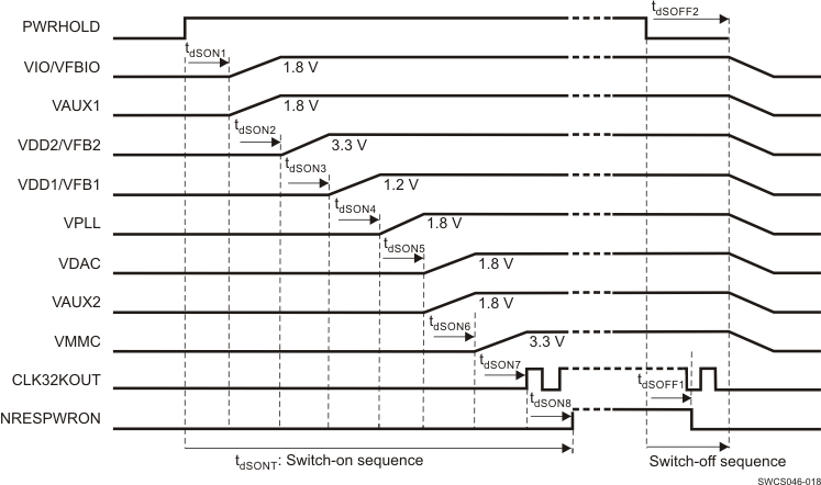 Figure 5-1 Boot Mode: BOOT1 = 0, BOOT0 = 0
Table 5-2 lists the 00 Boot mode timing characteristics.
Table 5-2 Boot Mode: BOOT1 = 0, BOOT0 = 0 Timing Characteristics
| PARAMETER | TEST CONDITIONS | MIN | TYP | MAX | UNIT |
|---|---|---|---|---|---|
| tdSON1 | PWRHOLD rising edge to VIO, VAUX1 enable delay | 66 × tCK32k = 2060 | µs | ||
| tdSON2 | VIO to VDD2 enable delay | 64 × tCK32k = 2000 | µs | ||
| tdSON3 | VDD2 to VDD1 enable delay | 64 × tCK32k = 2000 | µs | ||
| tdSON4 | VDD1 to VPLL enable delay | 64 × tCK32k = 2000 | µs | ||
| tdSON5 | VPLL to VDAC,VAUX2 enable delay | 64 × tCK32k = 2000 | µs | ||
| tdSON6 | VDAC to VMMC enable delay | 64 × tCK32k = 2000 | µs | ||
| VMMC to CLK32KOUT rising edge delay | 64 × tCK32k = 2000 | µs | |||
| tdSON8 | CLK32KOUT to NRESPWRON rising edge delay | 64 × tCK32k = 2000 | µs | ||
| tdSONT | Total switch-on delay | 16 | ms | ||
| tdSOFF1 | PWRHOLD falling edge to NRESPWRON falling edge delay | 2 × tCK32k = 62.5 | µs | ||
| tdSOFF1B | NRESPWRON falling edge to CLK32KOUT low delay | 3 × tCK32k = 92 | µs | ||
| tdSOFF2 | PWRHOLD falling edge to supplies and reference disable delay | 5 × tCK32k = 154 | µs |
Registers default setting: CK32K_CTRL = 1 (32-kHz RC oscillator is used), RTC_PWDN = 1 (RTC domain off), IT_POL = 0 (INt2 interrupt flag active low), VMBHI_IT_MSK = 0 (automatic switch-on on Battery plug), VMBCH_SEL = 11.
5.22.1.2 BOOT1 = 0, BOOT0 = 1
Table 5-3 provides details about the EEPROM setting for the BOOT modes. The power-up sequence for this boot mode is provided in Figure 5-2.
Table 5-3 Fixed Boot Mode: 01
| Register | Bit | Description | TPS65910 Boot 01 |
|---|---|---|---|
| VDD1_OP_REG | SEL | VDD1 voltage level selection for boot | 1.2 V |
| VDD1_REG | VGAIN_SEL | VDD1 Gain selection, x1 or x2 | x1 |
| EEPROM | VDD1 time slot selection | 3 | |
| DCDCCTRL_REG | VDD1_PSKIP | VDD1 pulse skip mode enable | Skip enabled |
| VDD2_OP_REG/VDD2_SR_REG | SEL | VDD2 voltage level selection for boot | 1.2 V |
| VDD2_REG | VGAIN_SEL | VDD2 Gain selection, x1 or x3 | x1 |
| EEPROM | VDD2 time slot selection | 4 | |
| DCDCCTRL_REG | VDD2_PSKIP | VDD2 pulse skip mode enable | Skip enabled |
| VIO_REG | SEL | VIO voltage selection | 1.8 V |
| EEPROM | VIO time slot selection | 1 | |
| DCDCCTRL_REG | VIO_PSKIP | VIO pulse skip mode enable | Skip enabled |
| EEPROM | VDD3 time slot | OFF | |
| VDIG1_REG | SEL | LDO voltage selection | 1.2 V |
| EEPROM | LDO time slot | OFF | |
| VDIG2_REG | SEL | LDO voltage selection | 1.0 V |
| EEPROM | LDO time slot | OFF | |
| VDAC_REG | SEL | LDO voltage selection | 1.8 V |
| EEPROM | LDO time slot | OFF | |
| VPLL_REG | SEL | LDO voltage selection | 1.8 V |
| EEPROM | LDO time slot | 2 | |
| VAUX1_REG | SEL | LDO voltage selection | 1.8 V |
| EEPROM | LDO time slot | OFF | |
| VMMC_REG | SEL | LDO voltage selection | 1.8 V |
| EEPROM | LDO time slot | OFF | |
| VAUX33_REG | SEL | LDO voltage selection | 3.3 V |
| EEPROM | LDO time slot | 6 | |
| VAUX2_REG | SEL | LDO voltage selection | 1.8 V |
| EEPROM | LDO time slot | 5 | |
| CLK32KOUT pin | CLK32KOUT time slot | 7 | |
| NRESPWRON pin | NRESPWRON time slot | 7+1 | |
| VRTC_REG | VRTC_OFFMASK | 0: VRTC LDO will be in low-power mode during OFF state | low-power mode |
| 1: VRC LDO will be in full-power mode during OFF state | |||
| DEVCTRL_REG | RTC_PWDN | 0: RTC in normal power mode | 1 |
| 1: Clock gating of RTC register and logic, low-power mode | |||
| DEVCTRL_REG | CK32K_CTRL | 0: Clock source is crystal/external clock | Crystal |
| 1: Clock source is internal RC oscillator | |||
| DEVCTRL2_REG | TSLOT_LENGTH[0] | Boot sequence time slot duration: | 2 ms |
| 0: 0.5 ms | |||
| 1: 2 ms | |||
| DEVCTRL2_REG | IT_POL | 0: INT1 signal will be active-low | Active-low |
| 1: INT1 signal will be active-high | |||
| INT_MSK_REG | VMBHI_IT_MSK | 0: Device will automatically switch-on at NOSUPPLY to OFF or BACKUP to OFF transition | 0: Automatic switch-on from supply insertion |
| 1: Startup reason required before switch-on | |||
| VMBCH_REG | VMBCH_SEL[1:0] | Select threshold for main battery comparator threshold VMBCH. | 3 V |
Figure 5-2 shows the 01 Boot mode timing characteristics.
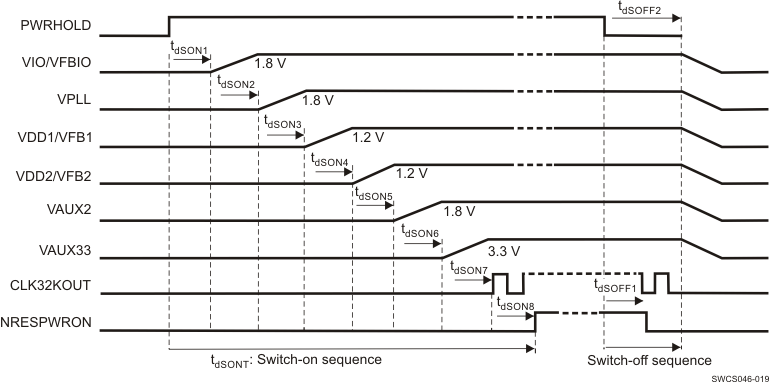 Figure 5-2 Boot Mode: BOOT1 = 0, BOOT0 = 1
Table 5-4 lists the 01 Boot mode timing characteristics.
Table 5-4 Boot Mode: BOOT1 = 0, BOOT0 = 1 Timing Characteristics
| PARAMETER | TEST CONDITIONS | MIN | TYP | MAX | UNIT |
|---|---|---|---|---|---|
| tdSON1 | PWRHOLD rising edge to VIO enable delay | 66 × tCK32k = 2060 | µs | ||
| tdSON2 | VIO to VPLL enable delay | 64 × tCK32k = 2000 | µs | ||
| tdSON3 | VPLL to VDD1 enable delay | 64 × tCK32k = 2000 | µs | ||
| tdSON4 | VDD1 to VDD2 enable delay | 64 × tCK32k = 2000 | µs | ||
| tdSON5 | VDD2 to VAUX2 enable delay | 64 × tCK32k = 2000 | µs | ||
| tdSON6 | VAUX2 to VAUX33 enable delay | 64 × tCK32k = 2000 | µs | ||
| tdSON7 | VAUX33 to CLK32KOUT enable delay | 64 × tCK32k = 2000 | µs | ||
| tdSON8 | CLK32KOUT to NRESPWRON enable delay | 64 × tCK32k = 2000 | µs | ||
| tdSONT | Total switch-on delay | 16 | ms | ||
| tdSOFF1 | PWRHOLD falling edge to NRESPWRON falling edge | 2 × tCK32k = 62.5 | µs | ||
| tdSOFF1B | NRESPWRON falling edge to CLK32KOUT low delay | 3 × tCK32k = 92 | µs | ||
| tdSOFF2 | PWRHOLD falling edge to supplies disable delay | 5 × tCK32k = 154 | µs |
Registers default setting: CK32K_CTRL = 0 (32-kHz quartz or external bypass clock is used), RTC_PWDN = 1 (RTC domain off), IT_POL = 0 (INt2 interrupt flag active low), VMBHI_IT_MSK = 0 (automatic switch-on on battery plug), VMBCH_SEL = 11.
5.22.2 Power Control Timing
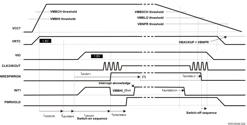
5.22.2.1 Device Turn-On/Off With Rising/Falling Input Voltage
Figure 5-3 shows the device turn-on/-off with rising/falling input voltage.
5.22.2.2 Device State Control Through PWRON Signal
Figure 5-4 shows the device state control through PWRON signal.
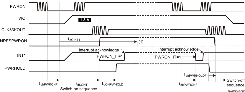
Figure 5-5 shows the long-press turn-off timing characteristics.
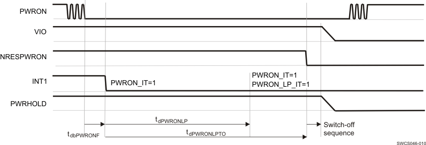
Table 5-5 lists the power control timing characteristics.
Table 5-5 Power Control Timing Characteristics
| PARAMETER | TEST CONDITIONS | MIN | TYP | MAX | UNIT |
|---|---|---|---|---|---|
| td32KON: 32-kHz Oscillator turn-on time | BOOT[1:0] = 00, RC oscillator | 0.1 | 2000 | ms | |
| BOOT[1:0] = 01, Quartz oscillator | 400 | ||||
| BOOT[1:0] = 01, Bypass clock | 0.1 | ||||
| tdbVMBHI: VMBHI rising-edge debouncing delay | 3 × tCK32k = 94 | 4 × tCK32k = 125 | µs | ||
| tdbVMBDCH: Main Battery voltage = VMBDCH threshold to INT1 falling-edge delay | 3 × tCK32k = 94 | 4 × tCK32k = 125 | s | ||
| tdbVMBLO: Main Battery voltage = VMBLO threshold to NRESPWRON falling-edge delay | 3 × tCK32k = 94 | 4 × tCK32k = 125 | s | ||
| tdbPWRONF: PWRON falling-edge debouncing delay | 500 | 550 | ms | ||
| tdbPWRONR: PWRON rising-edge debouncing delay | 3 × tCK32k= 94 | 4 × tCK32k = 125 | µs | ||
| tdbPWRHOLD: PWRON rising-edge debouncing delay | 2 × tCK32k = 63 | 3 × tCK32k= 94 | µs | ||
| tdOINT: INT1 (internal) Power-on pulse duration after PWRON low-level (debounced) event | 1 | s | |||
| tdONPWHOLD: delay to set high PWRHOLD signal or DEV_ON control bit after NRESPWRON released to keep on the supplies | 984 | ms | |||
| tdPWRONLP: PWRON long-press delay to interrupt | PWRON falling edge to PWON_LP_IT = 1 | 6 | s | ||
| tdPWRONLPTO: PWRON long-press delay to turn-off | PWRON falling edge to NRESPWRON falling edge | 8 | s |
5.22.2.3 Device SLEEP State Control
Figure 5-6 shows the device SLEEP state control timing characteristics.
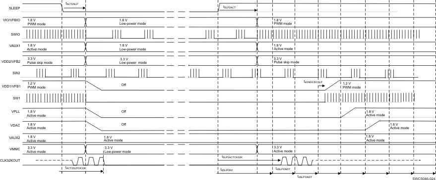
Table 5-6 Device SLEEP State Control Timing Characteristics
| PARAMETER | TEST CONDITIONS | MIN | TYP | MAX | UNIT |
|---|---|---|---|---|---|
| tACT2SLP | SLEEP falling edge to supply in low power mode (SLEEP resynchronization delay) |
2 × tCK32k = 62 | 3 × tCK32k = 94 | µs | |
| tACT2SLP | SLEEP falling edge to CLK32KOUT low | 156 | tACT2SLP + 3 × tCK32k | 188 | µs |
| tSLP2ACT | SLEEP rising edge to supply in high power mode | 8 × tCK32k = 250 | 9 × tCK32k = 281 | µs | |
| tSLP2ACTCK32K | SLEEP rising edge to CLK32KOUT running | 344 | tSLP2ACT + 3 × tCK32k | 375 | µs |
| tdSLPON1 | SLEEP rising edge to time step 1 of the tun-on sequence from SLEEP state | 281 | tSLP2ACT + 1 × tCK32k | 312 | µs |
| tdSLPONST | turn-on sequence step duration, from SLEEP state | µs | |||
| TSLOT_LENGTH[1:0] = 00 | 0 | ||||
| TSLOT_LENGTH[1:0] = 01 | 200 | ||||
| TSLOT_LENGTH[1:0] = 10 | 500 | ||||
| TSLOT_LENGTH[1:0] = 11 | 2000 | ||||
| tdSLPONDCDC | VDD1, VDD2 or VIO tun-on delay from tun-on sequence time step | 2 × tCK32k = 62 | us |
5.22.2.4 Power Supplies State Control Through the SCLSR_EN1 and SDASR_EN2 Signals
Figure 5-7 andFigure 5-8 show the power supplies state control through the SCLSR_EN1 and SDASR_EN2 signals timing characteristics.
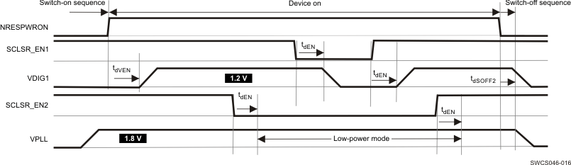
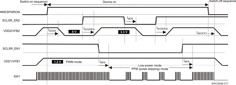
Table 5-7 Supplies State Control Though SCLSR_EN1 and SCLSR_EN2 Timing Characteristics
| PARAMETER | TEST CONDITIONS | MIN | TYP | MAX | UNIT |
|---|---|---|---|---|---|
| tdEN: NREPSWON to supply state change delay, SCLSR_EN1 or SCLSR_EN2 driven | 0 | ms | |||
| tdEN: SCLSR_EN1 or SCLSR_EN2 edge to supply state change delay | 1 × tCK32k = 31 | µs | |||
| tdVDDEN: SCLSR_EN1 or SCLSR_EN2 edge to VDD1 or VDD2 DC-DC turn on delay | 3 × tCK32k = 63 | µs |
5.22.2.5 VDD1 and VDD2 Voltage Control Through SCLSR_EN1 and SDASR_EN2 Signals
Figure 5-9 shows the VDD1 and VDD2 voltage control through the SCLSR_EN1 and SDASR_EN2 signals timing characteristics.
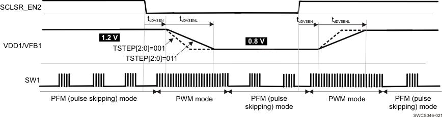
Table 5-8 VDD1 Supply Voltage Control Through SCLSR_EN1 Timing Characteristics
| PARAMETER | TEST CONDITIONS | MIN | TYP | MAX | UNIT |
|---|---|---|---|---|---|
| tdDVSEN: SCLSR_EN1 or SCLSR_EN2 edge to VDD1 or VDD2 voltage change delay | 2 × tCK32k = 62 | µs | |||
| tdDVSENL: VDD1 or VDD2 voltage settling delay | TSTEP[2:0] = 001 | 32 | µs | ||
| TSTEP[2:0] = 011 (default) | 0.4/7.5 = 53 | ||||
| TSTEP[2:0] = 111 | 160 |
5.22.2.6 SMPS Switching Synchronization
Figure 5-10 shows the SMPS switching synchronization timing characteristics.
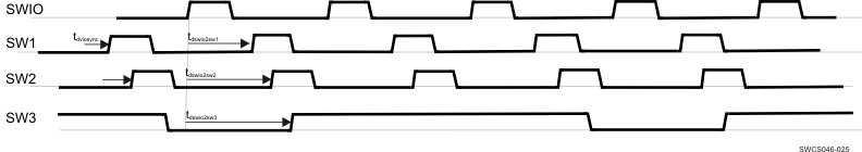
Table 5-9 SMPS Switching Synchronization Timing Characteristics
| PARAMETER | TEST CONDITIONS | MIN | TYP | MAX | UNIT |
|---|---|---|---|---|---|
| tdSWIO2SW1: delay from SWIO rising edge to SW1 rising edge | VDD1_PSKIP = 0, | ns | |||
| DCDCCKSYNC[1:0] = 11 | 160 | ||||
| DCDCCKSYNC[1:0] = 01 | 220 | ||||
| tdSWIO2SW2: delay from SWIO rising edge to SW1 rising edge | VDD2_PSKIP = 0, | ns | |||
| DCDCCKSYNC[1:0] = 11 | 160 | ||||
| DCDCCKSYNC[1:0] = 01 | 290 | ||||
| tdSWIO2SW3: delay from SWIO rising edge to SW3 rising edge | 206 | ns |