SWCS032F October 2008 – July 2014 TPS65950
PRODUCTION DATA.
- 1Device Overview
- 2Revision History
- 3Terminal Configuration and Functions
- 4Specifications
-
5Detailed Description
- 5.1
Power Module
- 5.1.1
Power Providers
- 5.1.1.1 VDD1 DC-DC Regulator
- 5.1.1.2 VDD2 DC-DC Regulator
- 5.1.1.3 VIO DC-DC Regulator
- 5.1.1.4 VDAC LDO Regulator
- 5.1.1.5 VPLL1 LDO Regulator
- 5.1.1.6 VPLL2 LDO Regulator
- 5.1.1.7 VMMC1 LDO Regulator
- 5.1.1.8 VMMC2 LDO Regulator
- 5.1.1.9 VSIM LDO Regulator
- 5.1.1.10 VAUX1 LDO Regulator
- 5.1.1.11 VAUX2 LDO Regulator
- 5.1.1.12 VAUX3 LDO Regulator
- 5.1.1.13 VAUX4 LDO Regulator
- 5.1.1.14 Internal LDOs
- 5.1.1.15 CP
- 5.1.1.16 USB LDO Short-Circuit Protection Scheme
- 5.1.2 Power References
- 5.1.3 Power Control
- 5.1.4 Power Consumption
- 5.1.5 Power Management
- 5.1.1
Power Providers
- 5.2 Real-Time Clock and Embedded Power Controller
- 5.3
Audio/Voice Module
- 5.3.1 Audio/Voice Downlink (RX) Module
- 5.3.2
Audio/Voice Uplink (TX) Module
- 5.3.2.1 Microphone Bias Module
- 5.3.2.2 Stereo Differential Input
- 5.3.2.3 Headset Differential Input
- 5.3.2.4 FM Radio/Auxiliary Stereo Input
- 5.3.2.5 PDM Interface for Digital Microphones
- 5.3.2.6 Uplink Characteristics
- 5.3.2.7 Microphone Amplification Stage
- 5.3.2.8 Carkit Input
- 5.3.2.9 Digital Audio Filter Module
- 5.3.2.10 Digital Voice Filter Module
- 5.4
USB HS 2.0 OTG Transceiver
- 5.4.1 USB Features
- 5.4.2
USB Transceiver
- 5.4.2.1 MCPC Carkit Port Timing
- 5.4.2.2 USB-CEA Carkit Port Timing
- 5.4.2.3 HS USB Port Timing
- 5.4.2.4
PHY Electrical Characteristics
- 5.4.2.4.1 5-V Tolerance
- 5.4.2.4.2 LS/FS Single-Ended Receivers
- 5.4.2.4.3 LS/FS Differential Receiver
- 5.4.2.4.4 LS/FS Differential Transmitter
- 5.4.2.4.5 HS Differential Receiver
- 5.4.2.4.6 HS Differential Transmitter
- 5.4.2.4.7 CEA/MCPC/UART Driver
- 5.4.2.4.8 Pullup/Pulldown Resistors
- 5.4.2.4.9 PHY DPLL Electrical Characteristics
- 5.4.2.4.10 PHY Power Consumption
- 5.4.2.5 OTG Electrical Characteristics
- 5.5 Battery Interface
- 5.6 MADC
- 5.7 LED Drivers
- 5.8 Keyboard
- 5.9 Clock Specifications
- 5.10 Debouncing Time
- 5.11 External Components
- 5.1
Power Module
- 6Device and Documentation Support
パッケージ・オプション
デバイスごとのパッケージ図は、PDF版データシートをご参照ください。
メカニカル・データ(パッケージ|ピン)
- ZXN|209
サーマルパッド・メカニカル・データ
発注情報
5 Detailed Description
5.1 Power Module
This section describes the electrical characteristics of the voltage regulators and timing characteristics of the supplies digitally controlled in the TPS65950.
Figure 5-1 is a block diagram of the power provider.
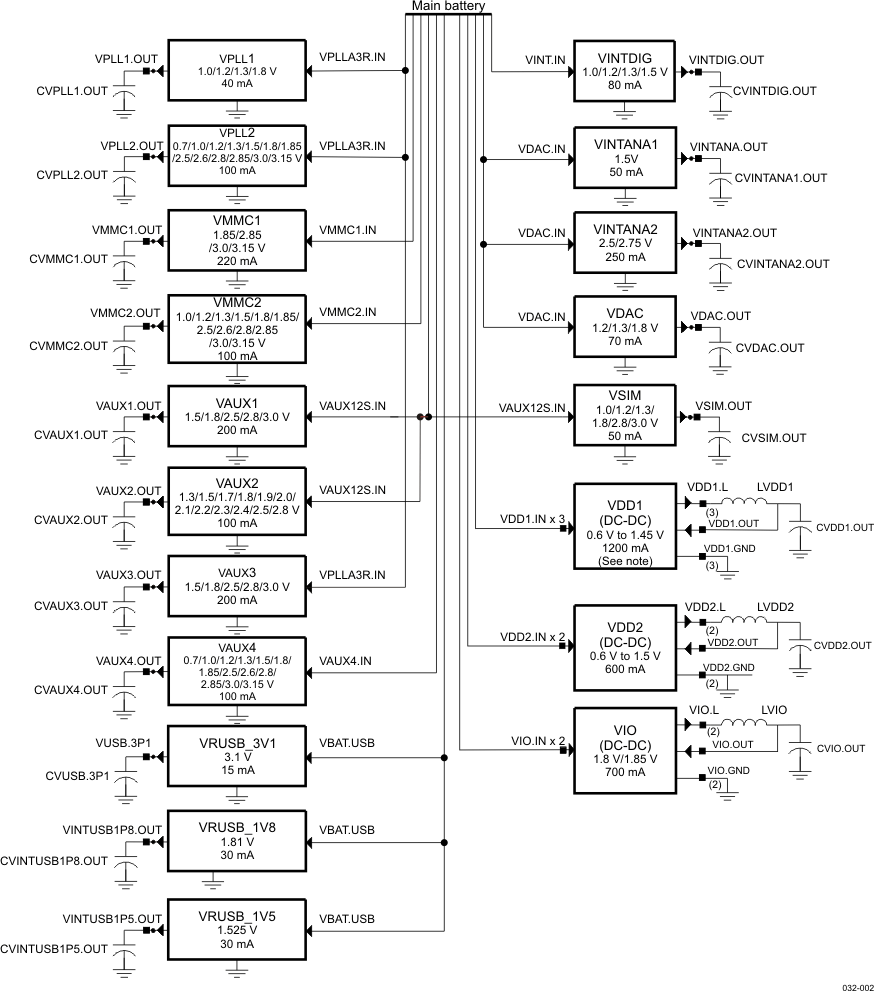
NOTE
For the component values, see Table 5-92.
5.1.1 Power Providers
Table 5-1 lists the power providers.
Table 5-1 Summary of the Power Providers
| Name | Use | Type | Voltage Range (V) | Default Voltage Depending on Boot Mode(1) |
Maximum Current | |||
|---|---|---|---|---|---|---|---|---|
| OMAP2 Mode | OMAP3 Mode | |||||||
| VAUX1 | External | LDO | 1.5, 1.8, 2.5, 2.8, 3.0 | 3.0 V | 3.0 V | 200 mA | ||
| VAUX2 | External | LDO | 1.3, 1.5, 1.7, 1.8, 1.9, 2.0, 2.1, 2.2, 2.3, 2.4, 2.5, 2.8 | 2.8 V | 1.8 V | 100 mA | ||
| VAUX3 | External | LDO | 1.5, 1.8, 2.5, 2.8, 3.0 | 2.8 V | 2.8 V | 200 mA | ||
| VAUX4 | External | LDO | 0.7, 1.0, 1.2, 1.3 1.5, 1.8, 1.85, 2.5, 2.6, 2.8, 2.85, 3.0, 3.15 | 1.2 V | 2.8 V | 100 mA | ||
| VMMC1 | External | LDO | 1.85, 2.85, 3.0, 3.15 | 1.85 V | 3.0 V | 220 mA | ||
| VMMC2 | External | LDO | 1.0, 1.2, 1.3, 1.5, 1.8, 1.85, 2.5, 2.6, 2.8, 2.85, 3.0, 3.15 | 2.6 V | 2.6 V | 100 mA | ||
| VPLL1 | External | LDO | 1.0, 1.2, 1.3, 1.8, 2.8, 3.0 | 1.3 V | 1.8 V | 40 mA | ||
| VPLL2 | External | LDO | 0.7, 1.0, 1.2, 1.3, 1.5, 1.8, 1.85, 2.5, 2.6, 2.8, 2.85, 3.0, 3.15 | 1.3 V | 1.3 V | 100 mA | ||
| VSIM | External | LDO | 1.0, 1.2, 1.3, 1.8, 2.8, 3.0 | 1.8 V | 1.8 V | 50 mA | ||
| VDAC | External | LDO | 1.2, 1.3, 1.8 | 1.8 V | 1.8 V | 70 mA | ||
| VIO | External | SMPS | 1.8, 1.85 | 1.8 V | 1.8 V | 700 mA | ||
| VDD1 for TPS65950A2/ TPS65950A3 |
External | SMPS | 0.6 ... 1.45 | 1.3 V | 1.2 V | 1200 mA | ||
| VDD1 for TPS65950A3 | External | SMPS | 1.2 ... 1.45 | 1.3 V | 1.2 V | 1400mA | ||
| VDD2 | External | SMPS | 0.6 ... 1.5 | 1.3 V | 1.2 V | 600 mA | ||
| VINTANA1 | Internal | LDO | 1.5 | 1.5 V | 1.5 V | 50 mA | ||
| VINTANA2 | Internal | LDO | 2.5, 2.75 | 2.75 V | 2.75 V | 250 mA | ||
| VINTDIG | Internal | LDO | 1.0, 1.2, 1.3, 1.5 | 1.5 V | 1.5 V | 80 mA | ||
| USBCP | Internal | CP | 5 | 5 V | 5 V | 100 mA | ||
| VUSB1V5 | Internal | LDO | 1.5 | 1.5 V | 1.5 V | 30 mA | ||
| VUSB1V8 | Internal | LDO | 1.8 | 1.8 V | 1.8 V | 30 mA | ||
| VUSB3V1 | Internal | LDO | 3.1 | 3.1 V | 3.1 V | 15 mA | ||
| VRRTC | Internal | LDO | 1.5 | 1.5 V | 1.5 V | 30 mA | ||
| VBRTC | Internal | LDO | 1.3 | 1.3 V | 1.3 V | 100 μA | ||
5.1.1.1 VDD1 DC-DC Regulator
5.1.1.1.1 VDD1 DC-DC Regulator Characteristics
The VDD1 DC-DC regulator is a stepdown DC-DC converter with a configurable output voltage. The programming of the output voltage and the characteristics of the DC-DC converter are SmartReflex-compatible. The regulator can be put in sleep mode to reduce its leakage (PFM) or power-down mode when it is not being used. Table 5-3 lists the characteristics of the regulator.
Table 5-2 Part Names With Corresponding VDD1 Current Support
| Device Name | VDD1 Current Support |
|---|---|
| TPS65950A2ZXN/R (some bug fixes, see errata) | 1.2 A |
| TPS65950A3ZXN/R (same as TPS65950A2 + 1 GHz support with higher current support) | 1.4 A |
Table 5-3 VDD1 DC-DC Regulator Characteristics
| Parameter | Comments | Min | Typ | Max | Unit |
|---|---|---|---|---|---|
| Input voltage range | 2.7 | 3.6 | 4.5 | V | |
| Output voltage | 0.6 | 1.45 | V | ||
| Output voltage step | Covering the 0.6 to 1.45-V range | 12.5 | mV | ||
| Output accuracy(1) | 0.6 to < 0.8 V | –6% | 6% | ||
| 0.8 to 1.45 V | –4% | 4% | |||
| Switching frequency | 3.2 | MHz | |||
| Conversion efficiency(2), Figure 5-2 in active and sleep modes | IO = 10 mA, sleep | 82% | |||
| 100 mA < IO < 400 mA | 85% | ||||
| 400 mA < IO < 600 mA | 80% | ||||
| 600 mA < IO < 800 mA | 75% | ||||
| Output current | Active mode, Output Voltage 0.6 V to 1.45 V for TPS65950A2/TPS65950A3 | 1200 | mA | ||
| Active mode, Output Voltage 1.2 V to1.45 V for TPS65950A3 | 1400 | mA | |||
| Sleep mode | 10 | mA | |||
| Ground current (IQ) | Off at 30°C | 3 | μA | ||
| Sleep, unloaded | 30 | 50 | |||
| Active, unloaded, not switching | 300 | ||||
| Short-circuit current | VIN = VMax | 2.2 | A | ||
| Load regulation | 0 < IO < IMax | 20 | mV | ||
| Transient load regulation(3) | IO = 10 mA to 600 +10 mA, Maximum slew rate is 600mA/100 ns. |
–65 | 50 | mV | |
| Line regulation | 10 | mV | |||
| Transient line regulation | 300 mVPP ac input, 10-μs rise and fall time | 10 | mV | ||
| Startup time | 0.25 | 1 | ms | ||
| Recovery time | From sleep mode to on mode with constant load | <10 | 100 | μs | |
| Slew rate (rising or falling)(4) | 4 | 8 | 16 | mV/μs | |
| Output shunt resistor (pulldown) | 500 | 700 | Ω | ||
| External coil | Value | 0.7 | 1 | 1.3 | μH |
| DCR | 0.1 | Ω | |||
| Saturation current for TPS65950A2 | 1.8 | A | |||
| Saturation current for TPS65950A3 | 2.1 | ||||
| External capacitor(1) | Value | 8 | 10 | 12 | μF |
| Equivalent series resistance (ESR) at switching frequency | 0 | 20 | mΩ |
Transient load is specified at Vout max with a ±50% external capacitor accuracy and includes temperature and process variation.
See Table 3-2 for how to connect the VDD1/2 DC-DC converter when it is not used.
Figure 5-2 shows the efficiency of the VDD1 DC-DC regulator in active and sleep modes.
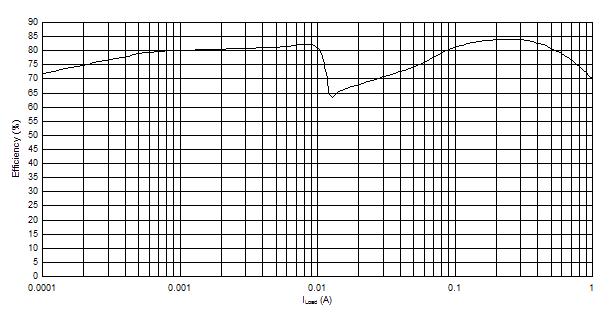 Figure 5-2 VDD1 DC-DC Regulator Efficiency – Output Voltage = 1.3 V, VBAT = 3.6 V
5.1.1.1.2 External Components and Application Schematic
Figure 5-3 is an application schematic with the external components on the VDD1 DC-DC regulator.
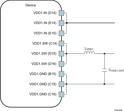 Figure 5-3 VDD1 DC-DC Application Schematic
NOTE
For the component values, see Table 5-92.
5.1.1.2 VDD2 DC-DC Regulator
5.1.1.2.1 VDD2 DC-DC Regulator Characteristics
The VDD2 DC-DC regulator is a programmable output stepdown DC-DC converter with an internal field effect transistor (FET). Like the VDD1 regulator, the VDD2 regulator can be placed in sleep or power-down mode and is SmartReflex-compatible. The VDD2 regulator differs from VDD1 in its current load capability. Table 5-4 lists the characteristics of the regulator.
Table 5-4 VDD2 DC-DC Regulator Characteristics
| Parameter | Comments | Min | Typ | Max | Unit |
|---|---|---|---|---|---|
| Input voltage range | 2.7 | 3.6 | 4.5 | V | |
| Output voltage | 0.6 | 1 | 1.5 | V | |
| Output voltage step | Covering the 0.6-V to 1.45-V range, 1.5 V is a single programmable value. |
12.5 | mV | ||
| Output accuracy(1) | 0.6 to < 0.8 V | –6% | 6% | ||
| 0.8 o 1.5 V | –4% | 4% | |||
| Switching frequency | 3.2 | MHz | |||
| Conversion efficiency(2), Figure 5-4 in active mode and sleep mode | IO = 10 mA, sleep | 82% | |||
| 100 mA < IO < 300 mA | 85% | ||||
| 300 mA < IO < 500 mA | 80% | ||||
| Output current | Active mode | 700 | mA | ||
| Sleep mode | 10 | ||||
| Ground current (IQ) | Off at 30°C | 1 | μA | ||
| Sleep, unloaded | 50 | ||||
| Active, unloaded, not switching | 300 | ||||
| Short-circuit current | VIN = VMax | 1.2 | A | ||
| Load regulation | 0 < IO < IMax | 20 | mV | ||
| Transient load regulation(3) | IO = 10 mA to (IMax/2) + 10 mA, Maximum slew rate is IMax/2/100 ns. |
–65 | 50 | mV | |
| Line regulation | 10 | mV | |||
| Transient line regulation | 300 mVPP ac input, 10-μs rise and fall time | 10 | mV | ||
| Output shunt resistor (internal pulldown) | 500 | 700 | Ω | ||
| Startup time | 0.25 | 1 | ms | ||
| Recovery time | From sleep mode to on mode with constant load | 25 | 100 | μs | |
| Slew rate (rising or falling)(4) | 4 | 8 | 16 | mV/μs | |
| External coil | Value | 0.7 | 1 | 1.3 | μH |
| DCR | 0.1 | Ω | |||
| Saturation current | 900 | mA | |||
| External capacitor(5) | Value | 8 | 10 | 12 | μF |
| ESR at switching frequency | 0 | 20 | mΩ |
Imax/2 (300 mA) in 100 ns with a ±20% external capacitor accuracy or
Imax/3 (200 mA) in 100 ns with a ±50% external capacitor accuracy
See Table 3-2 for how to connect the VDD2 DC-DC converter when it is not used.
Figure 5-4 shows the efficiency of the VDD2 DC-DC regulator in active and sleep modes.
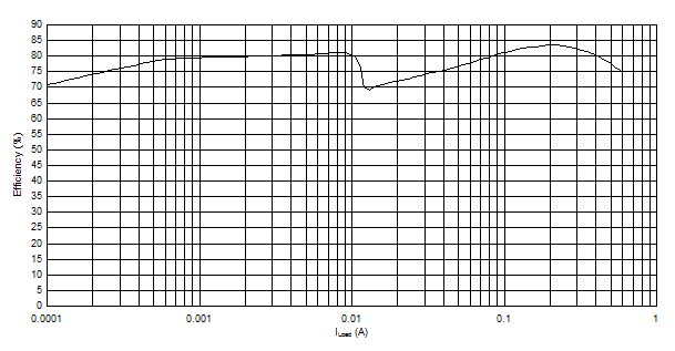 Figure 5-4 VDD2 DC-DC Regulator Efficiency – Output Voltage = 1.3 V, VBAT = 3.6 V
5.1.1.2.2 External Components and Application Schematic
Figure 5-5 is an application schematic with the external components of the VDD2 DC-DC regulator.
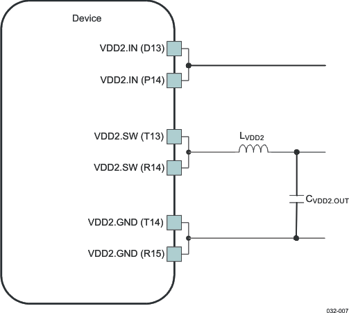 Figure 5-5 VDD2 DC-DC Application Schematic
NOTE
For the component values, see Table 5-92.
5.1.1.3 VIO DC-DC Regulator
5.1.1.3.1 VIO DC-DC Regulator Characteristics
The I/Os and memory DC-DC regulator is a 600-mA stepdown DC-DC converter (internal FET) with two output voltage settings. It supplies the memories and all I/O ports in the application and is one of the first power providers to switch on in the power-up sequence. This DC-DC regulator can be placed in sleep or power-down mode; however, care must be taken in the sequencing of this power provider, because numerous electrostatic discharge (ESD) blocks are connected to this supply. Table 5-5 lists the characteristics of the regulator.
Table 5-5 VIO DC-DC Regulator Characteristics
| Parameter | Comments | Min | Typ | Max | Unit |
|---|---|---|---|---|---|
| Input voltage range | 2.7 | 3.6 | 4.5 | V | |
| Output voltage(1) | 1.8 1.85 |
V | |||
| Output accuracy (2) | –4% | 4% | |||
| –3% | 3% | ||||
| Switching frequency | 3.2 | MHz | |||
| Conversion efficiency(3)Figure 5-6 in active mode and sleep modes | IO = 10 mA, sleep | 85% | |||
| 100 mA < IO < 400 mA | 85% | ||||
| 400 mA < IO < 600 mA | 80% | ||||
| Output current | On mode | 700 | mA | ||
| Sleep mode | 10 | ||||
| Ground current (IQ) | Off at 30°C | 1 | μA | ||
| Sleep, unloaded | 50 | ||||
| Active, unloaded, not switching | 300 | ||||
| Load transient(4) | 50 | mV | |||
| Line transient | 300 mVPP ac, input rise and fall time 10 μs | 10 | mV | ||
| Start-up time | 0.25 | 1 | ms | ||
| Recovery time | From sleep mode to on mode with constant load | <10 | 100 | μs | |
| Output shunt resistor (internal pulldown) | 500 | 700 | Ω | ||
| External coil | Value | 0.7 | 1 | 1.3 | μH |
| DCR | 0.1 | Ω | |||
| Saturation current | 900 | mA | |||
| External capacitor | Value | 8 | 10 | 12 | μF |
| ESR at switching frequency | 1 | 20 | mΩ |
±3% accuracy is dc accuracy only.
Figure 5-6 shows the efficiency of the VIO DC-DC regulator in active and sleep modes.
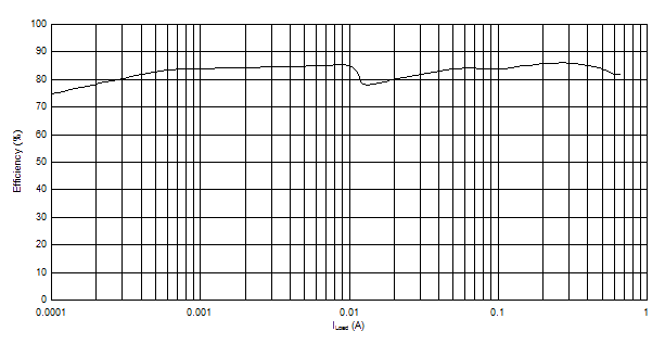 Figure 5-6 VIO DC-DC Regulator Efficiency in Active Mode – Output Voltage = 1.2 V, VBAT = 3.8 V
5.1.1.3.2 External Components and Application Schematic
Figure 5-7 is an application schematic with the external components of the VIO DC-DC regulator.
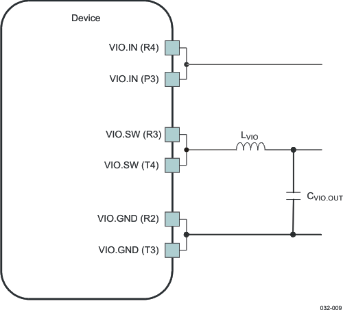 Figure 5-7 VIO DC-DC Application Schematic
NOTE
For the component values, see Table 5-92.
5.1.1.4 VDAC LDO Regulator
The VDAC programmable LDO regulator is a high power-supply ripple rejection (PSRR), low-noise, linear regulator that powers the host processor dual-video DAC. It is controllable with registers through I2C and can be powered down. Table 5-6 lists the characteristics of the regulator.
Table 5-6 VDAC LDO Regulator Characteristics
| Parameter | Test Conditions | Min | Typ | Max | Unit | |
|---|---|---|---|---|---|---|
| Output Load Conditions | ||||||
| Filtering capacitor | Connected from VDAC.OUT to analog ground | 0.3 | 1 | 2.7 | μF | |
| Filtering capacitor ESR | 20 | 600 | mΩ | |||
| Electrical Characteristics | ||||||
| VIN | Input voltage | 2.7 | 3.6 | 4.5 | V | |
| VOUT | Output voltage | On mode | 1.164 | 1.2 | 1.236 | V |
| 1.261 | 1.3 | 1.339 | ||||
| 1.746 | 1.8 | 1.854 | ||||
| IOUT | Rated output current | On mode | 70 | mA | ||
| Low-power mode | 5 | |||||
| dc load regulation | On mode: 0 < IO < IMax | 20 | mV | |||
| dc line regulation | On mode, VIN = VINmin to VINmax at IOUT = IOUTmax | 3 | mV | |||
| Turn-on time | IOUT = 0, CL = 1 μF (within 10% of VOUT) | 100 | μs | |||
| Wake-up time | Full load capability | 10 | μs | |||
| Ripple rejection | f < 20 kHz | 65 | dB | |||
| 20 kHz < f < 100 kHz | 45 | |||||
| f = 1 MHz | 40 | |||||
| VIN = VOUT + 1 V, IO = IMax | ||||||
| Output noise | 100 Hz < f < 5 kHz | 400 | nV/√Hz | |||
| 5 kHz < f < 400 kHz | 125 | |||||
| 400 kHz < f < 10 MHz | 50 | |||||
| Ground current | On mode, IOUT = 0 | 150 | μA | |||
| On mode, IOUT = IOUTmax | 350 | |||||
| Low-power mode, IOUT = 0 | 15 | |||||
| Low-power mode, IOUT = 1 mA | 25 | |||||
| Off mode at 55°C | 1 | |||||
| VDO | Dropout voltage | On mode, IOUT = IOUTmax | 250 | mV | ||
| Transient load regulation | ILoad: IMin – IMax
Slew: 60 mA/μs |
–40 | 40 | mV | ||
| Transient line regulation | VIN drops 500 mV Slew: 40 mV/μs |
10 | mV | |||
5.1.1.5 VPLL1 LDO Regulator
The VPLL1 programmable LDO regulator is high-PSRR, low-noise, linear regulator used for the host processor phase-locked loop (PLL) supply. Table 5-7 lists the characteristics of the regulator.
Table 5-7 VPLL1 LDO Regulator Characteristics
| Parameter | Test Conditions | Min | Typ | Max | Unit | |
|---|---|---|---|---|---|---|
| Output Load Conditions | ||||||
| Filtering capacitor | Connected from VPLL1.OUT to analog ground | 0.3 | 1 | 2.7 | μF | |
| Filtering capacitor ESR | 20 | 600 | mΩ | |||
| Electrical Characteristics | ||||||
| VIN | Input voltage | 2.7 | 3.6 | 4.5 | V | |
| VOUT | Output voltage | On mode and low-power mode | 0.97 | 1.0 | 1.03 | V |
| 1.164 | 1.2 | 1.236 | ||||
| 1.261 | 1.3 | 1.339 | ||||
| 1.746 | 1.8 | 1.854 | ||||
| 2.716 | 2.8 | 2.884 | ||||
| 2.91 | 3.0 | 3.090 | ||||
| IOUT | Rated output current | On mode | 40 | mA | ||
| Low-power mode | 5 | |||||
| dc load regulation | On mode: 0 < IO < IMax | 20 | mV | |||
| dc line regulation | On mode, VIN = VINmin to VINmax at IOUT = IOUTmax | 3 | mV | |||
| Turn-on time | IOUT = 0, CL = 1 μF (within 10% of VOUT) | 100 | μs | |||
| Wake-up time | Full load capability | 10 | μs | |||
| Ripple rejection | f < 10 kHz | 50 | dB | |||
| 10 kHz < f < 100 kHz | 40 | |||||
| f = 1 MHz | 30 | |||||
| VIN = VOUT + 1 V, IO = IMax | ||||||
| Ground current | On mode, IOUT = 0 | 70 | μA | |||
| On mode, IOUT = IOUTmax | 110 | |||||
| Low-power mode, IOUT = 0 | 15 | |||||
| Low-power mode, IOUT = 1 mA | 16 | |||||
| Off mode at 55°C | 1 | |||||
| VDO | Dropout voltage | On mode, IOUT = IOUTmax | 250 | mV | ||
| Transient load regulation | ILoad: IMin – IMax
Slew: 60 mA/μs |
–40 | 40 | mV | ||
| Transient line regulation | VIN drops 500 mV Slew: 40 mV/μs |
10 | mV | |||
5.1.1.6 VPLL2 LDO Regulator
The VPLL2 programmable LDO regulator is a high-PSRR, low-noise, linear regulator used for the host processor PLL supply. Table 5-8 lists the characteristics of the regulator.
Table 5-8 VPLL2 LDO Regulator Characteristics
| Parameter | Test Conditions | Min | Typ | Max | Unit | |
|---|---|---|---|---|---|---|
| Output Load Conditions | ||||||
| Filtering capacitor | Connected from VPLL2.OUT to analog ground | 0.3 | 1 | 2.7 | μF | |
| Filtering capacitor ESR | 20 | 600 | mΩ | |||
| Electrical Characteristics | ||||||
| VIN | Input voltage | 2.7 | 3.6 | 4.5 | V | |
| VOUT | Output voltage | On mode and low-power mode | 0.672 0.97 1.164 1.261 1.455 1.746 1.795 2.425 2.522 2.716 2.765 2.91 3.05 |
0.7 1.0 1.2 1.3 1.5 1.8 1.85 2.5 2.6 2.8 2.85 3.0 3.15 |
0.728 1.03 1.236 1.339 1.545 1.854 1.906 2.575 2.678 2.884 2.936 3.09 3.245 |
V |
| IOUT | Rated output current | On mode Low-power mode |
100 5 |
mA | ||
| dc load regulation | On mode: 0 < IO < IMax | 20 | mV | |||
| dc line regulation | On mode, VIN = VINmin to VINmax at IOUT = IOUTmax | 3 | mV | |||
| Turn-on time | IOUT = 0, CL = 1 μF (within 10% of VOUT) | 100 | μs | |||
| Wake-up time | Full load capability | 10 | μs | |||
| Ripple rejection | f < 10 kHz 10 kHz < f < 100 kHz f = 1 MHz VIN = VOUT + 1 V, IO = IMax |
50 40 30 |
dB | |||
| Ground current | On mode, IOUT = 0 On mode, IOUT = IOUTmax Low-power mode, IOUT = 0 Low-power mode, IOUT = 1 mA Off mode at 55°C |
70 160 17 20 1 |
μA | |||
| VDO | Dropout voltage | On mode, IOUT = IOUTmax | 250 | mV | ||
| Transient load regulation | ILoad: IMin – IMax
Slew: 40 mA/μs |
–40 | 40 | mV | ||
| Transient line regulation | VIN drops 500 mV Slew: 40 mV/μs |
10 | mV | |||
5.1.1.7 VMMC1 LDO Regulator
The VMMC1 LDO regulator is a programmable linear voltage converter that powers the multimedia channel (MMC) slot. It includes a discharge resistor and overcurrent (short -ircuit) protection. This LDO regulator can also be turned off automatically when MMC card extraction is detected. The VMMC1 LDO can be powered through an independent supply other than the battery; for example, a charge pump (CP). In this case, the input from the VMMC1 LDO can be higher than the battery voltage. Table 5-9 lists the characteristics of the regulator.
Table 5-9 VMMC1 LDO Regulator Characteristics
| Parameter | Test Conditions | Min | Typ | Max | Unit | |
|---|---|---|---|---|---|---|
| Output Load Conditions | ||||||
| Filtering capacitor | Connected from VMMC1.OUT to analog ground | 0.3 | 1 | 2.7 | μF | |
| Filtering capacitor ESR | 20 | 600 | mΩ | |||
| Electrical Characteristics | ||||||
| VIN | Input voltage | 2.7 | 3.6 | 5.5 | V | |
| VOUT | Output voltage | On mode and low-power mode | 1.7945 2.7645 2.91 3.0555 |
1.85 2.85 3.0 3.15 |
1.9055 2.9355 3.09 3.2445 |
V |
| IOUT | Rated output current | On mode Low-power mode |
220 5 |
mA | ||
| dc load regulation | On mode: 0 < IO < IMax | 20 | mV | |||
| dc line regulation | On mode, VIN = VINmin to VINmax at IOUT = IOUTmax | 3 | mV | |||
| Turn-on time | IOUT = 0, CL = 1 μF (within 10% of VOUT) | 100 | μs | |||
| Wake-up time | Full load capability | 10 | μs | |||
| Ripple rejection | f < 10 kHz 10 kHz < f < 100 kHz f = 1 MHz VIN = VOUT + 1 V, IO = IMax |
50 40 25 |
dB | |||
| Ground current | On mode, IOUT = 0 On mode, IOUT = IOUTmax Low-power mode, IOUT = 0 Low-power mode, IOUT = 5 mA Off mode at 55°C |
70 290 17 20 1 |
μA | |||
| VDO | Dropout voltage | On mode, IOUT = IOUTmax | 250 | mV | ||
| Transient load regulation | ILoad: IMin – IMax
Slew: 40 mA/μs |
–40 | 40 | mV | ||
| Transient line regulation | VIN drops 500 mV Slew: 40 mV/μs |
10 | mV | |||
5.1.1.8 VMMC2 LDO Regulator
The VMMC2 LDO regulator is a programmable linear voltage converter that powers MMC slot 2. It includes a discharge resistor and overcurrent (short-circuit) protection. The VMMC2 LDO can be powered through an independent supply other than the battery (for example, a CP). In this case, the input from the VMMC2 LDO can be higher than the battery voltage. Table 5-10 lists the characteristics of the regulator.
Table 5-10 VMMC2 LDO Regulator Characteristics
| Parameter | Test Conditions | Min | Typ | Max | Unit | |
|---|---|---|---|---|---|---|
| Output Load Conditions | ||||||
| Filtering capacitor | Connected from VMMC2.OUT to analog ground | 0.3 | 1 | 2.7 | μF | |
| Filtering capacitor ESR | 20 | 600 | mΩ | |||
| Electrical Characteristics | ||||||
| VIN | Input voltage | 2.7 | 3.6 | 5.5 | V | |
| VOUT | Output voltage | On mode and low-power mode | 0.7 1.164 1.261 1.455 1.746 1.795 2.425 2.522 2.716 2.765 2.91 3.056 |
1.0 1.2 1.3 1.5 1.8 1.85 2.5 2.6 2.8 2.85 3.0 3.15 |
1.03 1.236 1.339 1.545 1.854 1.906 2.575 2.678 2.884 2.936 3.09 3.245 |
V |
| IOUT | Rated output current | On mode Low-power mode |
100 5 |
mA | ||
| dc load regulation | On mode: 0 < IO < IMax | 20 | mV | |||
| dc line regulation | On mode, VIN = VINmin to VINmax at IOUT = IOUTmax | 3 | mV | |||
| Turn-on time | IOUT = 0, CL = 1 μF (within 10% of VOUT) | 100 | μs | |||
| Wake-up time | Full load capability | 10 | μs | |||
| Ripple rejection | f < 10 kHz 10 kHz < f < 100 kHz f = 1 MHz VIN = VOUT + 1 V, IO = IMax |
50 40 30 |
dB | |||
| Ground current | On mode, IOUT = 0 On mode, IOUT = IOUTmax Low-power mode, IOUT = 0 Low-power mode, IOUT = 50 μA Off mode at 55°C |
70 170 17 20 1 |
μA | |||
| VDO | Dropout voltage | On mode, IOUT = IOUTmax | 250 | mV | ||
| Transient load regulation | ILoad: IMin – IMax
Slew: 40 mA/μs |
–40 | 40 | mV | ||
| Transient line regulation | VIN drops 500 mV Slew: 40 mV/μs |
10 | mV | |||
5.1.1.9 VSIM LDO Regulator
The VSIM voltage regulator is a programmable, low-dropout, linear voltage regulator that supplies the subscriber identity module (SIM)-card and the SIM-card driver. This LDO regulator can be turned off automatically when SIM card extraction is detected. Table 5-11 lists the characteristics of the regulator.
Table 5-11 VSIM LDO Regulator Characteristics
| Parameter | Test Conditions | Min | Typ | Max | Unit | |
|---|---|---|---|---|---|---|
| Output Load Conditions | ||||||
| Filtering capacitor | Connected from VSIM.OUT to analog ground | 0.3 | 1 | 2.7 | μF | |
| Filtering capacitor ESR | 20 | 600 | mΩ | |||
| Electrical Characteristics | ||||||
| VIN | Input voltage | 2.7 | 3.6 | 4.5 | V | |
| VOUT | Output voltage | On mode and low-power mode | 0.97 1.164 1.261 1.746 2.716 2.91 |
1.0 1.2 1.3 1.8 2.8 3.0 |
1.03 1.236 1.339 1.854 2.884 3.09 |
V |
| IOUT | Rated output current | On mode Low-power mode |
50 1 |
mA | ||
| dc load regulation | On mode: 0 < IO < IMax | 20 | mV | |||
| dc line regulation | On mode, VIN = VINmin to VINmax at IOUT = IOUTmax | 3 | mV | |||
| Turn-on time | IOUT = 0, CL = 1 μF (within 10% of VOUT) | 100 | μs | |||
| Wake-up time | Full load capability | 10 | μs | |||
| Ripple rejection | f < 10 kHz 10 kHz < f < 100 kHz f = 1 MHz VIN = VOUT + 1 V, IO = IMax |
50 40 30 |
dB | |||
| Ground current | On mode, IOUT = 0 On mode, IOUT = IOUTmax Low-power mode, IOUT = 0 Low-power mode, IOUT = 1 mA Off mode at 55°C |
70 120 15 16 1 |
μA | |||
| VDO | Dropout voltage | On mode, IOUT = IOUTmax | 250 | mV | ||
| Transient load regulation | ILoad: IMin – IMax
Slew: 40 mA/μs |
–40 | 40 | mV | ||
| Transient line regulation | VIN drops 500 mV Slew: 40 mV/μs |
10 | mV | |||
5.1.1.10 VAUX1 LDO Regulator
The VAUX1 GP LDO regulator powers the auxiliary devices. The VAUX1 regulator can also support an inductive load such as a vibrator. While operating in vibrator mode, the VAUX1 LDO has the following features:
- Programmable, register-controlled, soft-start function
- Enabled through the VIBRA.SYNC pin
- Programmable, register-controlled, duty cycle (PWM generator) based on a nominal 4-Hz cycle derived from an internal 32-kHz clock
Table 5-12 lists the characteristics of the regulator.
Table 5-12 VAUX1 LDO Regulator Characteristics
| Parameter | Test Conditions | Min | Typ | Max | Unit | |
|---|---|---|---|---|---|---|
| Output Load Conditions | ||||||
| Filtering capacitor | Connected from VAUX1.OUT to analog ground | 0.3 | 1 | 2.7 | μF | |
| Filtering capacitor ESR | 20 | 600 | mΩ | |||
| Vibrator inductive load(1) | Connected from VAUX1.OUT to analog ground | 70 | 700 | μH | ||
| Vibrator load resistance(1) | 15 | 50 | Ω | |||
| Electrical Characteristics | ||||||
| VIN | Input voltage | 2.7 | 3.6 | 4.5 | V | |
| VOUT | Output voltage | On mode and low-power mode | 1.455 1.746 2.425 2.716 2.91 |
1.5 1.8 2.5 2.8 3.0 |
1.545 1.854 2.575 2.884 3.09 |
V |
| IOUT | Rated output current | On mode Low-power mode |
200 5 |
mA | ||
| dc load regulation | On mode: IOUT = IOUTmax to 0 | 20 | mV | |||
| dc line regulation | On mode, VIN = VINmin to VINmax at IOUT = IOUTmax | 3 | mV | |||
| Turn-on time | IOUT = 0, CL = 1 μF (within 10% of VOUT) Soft-start function for inductive load |
100 500 |
μs | |||
| Turn-off time | 5000 | μs | ||||
| Wake-up time | Full load capability | 10 | μs | |||
| Ripple rejection | f < 10 kHz 10 kHz < f < 100 kHz f = 1 MHz VIN = VOUT + 1 V, IO = IMax |
50 40 25 |
dB | |||
| Ground current | On mode, IOUT = 0 On mode, IOUT = IOUTmax Low-power mode, IOUT = 0 Low-power mode, IOUT = 5 mA Off mode at 55°C |
70 270 15 20 1 |
μA | |||
| VDO | Dropout voltage | On mode, IOUT = IOUTmax | 250 | mV | ||
| Transient load regulation | ILoad: IMin – IMax
Slew: 40 mA/μs |
–40 | 40 | mV | ||
| Transient line regulation | VIN drops 500 mV Slew: 40 mV/μs |
10 | mV | |||
5.1.1.11 VAUX2 LDO Regulator
The VAUX2 GP LDO regulator powers the auxiliary devices. Table 5-13 lists the characteristics of the regulator.
Table 5-13 VAUX2 LDO Regulator Characteristics
| Parameter | Test Conditions | Min | Typ | Max | Unit | |
|---|---|---|---|---|---|---|
| Output Load Conditions | ||||||
| Filtering capacitor | Connected from VAUX2.OUT to analog ground | 0.3 | 1 | 2.7 | μF | |
| Filtering capacitor ESR | 20 | 600 | mΩ | |||
| Electrical Characteristics | ||||||
| VIN | Input voltage | 2.7 | 3.6 | 4.5 | V | |
| VOUT | Output voltage | On mode and low-power mode | –3% | 1.3 1.5 1.7 1.8 1.9 2.0 2.1 2.2 2.3 2.4 2.5 2.8 |
3% | V |
| IOUT | Rated output current | On mode Low-power mode |
100 5 |
mA | ||
| dc load regulation | On mode: IOUT = IOUTmax to 0 | 20 | mV | |||
| dc line regulation | On mode, VIN = VINmin to VINmax at IOUT = IOUTmax | 3 | mV | |||
| Turn-on time | IOUT = 0, CL = 1 μF (within 10% of VOUT) | 100 | μs | |||
| Wake-up time | Full load capability | 10 | μs | |||
| Ripple rejection | f < 10 kHz 10 kHz < f < 100 kHz f = 1 MHz VIN = VOUT + 1 V, IO = IMax |
50 40 25 |
dB | |||
| Ground current | On mode, IOUT = 0 On mode, IOUT = IOUTmax Low-power mode, IOUT = 0 Low-power mode, IOUT = 5 mA Off mode at 55°C |
70 170 17 20 1 |
μA | |||
| VDO | Dropout voltage | On mode, IOUT = IOUTmax | 250 | mV | ||
| Transient load regulation | ILoad: IMin – IMax
Slew: 40 mA/μs |
–40 | 40 | mV | ||
| Transient line regulation | VIN drops 500 mV Slew: 40 mV/μs |
10 | mV | |||
5.1.1.12 VAUX3 LDO Regulator
The VAUX3 GP LDO regulator powers the auxiliary devices. Table 5-14 lists the characteristics of the regulator.
Table 5-14 VAUX3 LDO Regulator Characteristics
| Parameter | Test Conditions | Min | Typ | Max | Unit | |
|---|---|---|---|---|---|---|
| Output Load Conditions | ||||||
| Filtering capacitor | Connected from VAUX3.OUT to analog ground | 0.3 | 1 | 2.7 | μF | |
| Filtering capacitor ESR | 20 | 600 | mΩ | |||
| Electrical Characteristics | ||||||
| VIN | Input voltage | 2.7 | 3.6 | 4.5 | V | |
| VOUT | Output voltage | On mode and low-power mode | 1.455 1.746 2.425 2.716 2.91 |
1.5 1.8 2.5 2.8 3.0 |
1.545 1.854 2.575 2.884 3.09 |
V |
| IOUT | Rated output current | On mode Low-power mode |
200 5 |
mA | ||
| dc load regulation | On mode: IOUT = IOUTmax to 0 | 20 | mV | |||
| dc line regulation | On mode, VIN = VINmin to VINmax at IOUT = IOUTmax | 3 | mV | |||
| Turn-on time | IOUT = 0, CL = 1 μF (within 10% of VOUT) | 100 | μs | |||
| Wake-up time | Full load capability | 10 | μs | |||
| Ripple rejection | f < 10 kHz 10 kHz < f < 100 kHz f = 1 MHz VIN = VOUT + 1 V, IO = IMax |
50 40 25 |
dB | |||
| Ground current | On mode, IOUT = 0 On mode, IOUT = IOUTmax Low-power mode, IOUT = 0 Low-power mode, IOUT = 5 mA Off mode at 55°C |
70 270 15 20 1 |
μA | |||
| VDO | Dropout voltage | On mode, IOUT = IOUTmax | 250 | mV | ||
| Transient load regulation | ILoad: IMin – IMax
Slew: 40 mA/μs |
–40 | 40 | mV | ||
| Transient line regulation | VIN drops 500 mV Slew: 40 mV/μs |
10 | mV | |||
5.1.1.13 VAUX4 LDO Regulator
The VAUX4 GP LDO regulator powers the auxiliary devices. The VAUX4 regulator has an independent supply input pin and can be preregulated by an external voltage. Table 5-15 lists the characteristics of the regulator.
Table 5-15 VAUX4 LDO Regulator Characteristics
| Parameter | Test Conditions | Min | Typ | Max | Unit | |
|---|---|---|---|---|---|---|
| Output Load Conditions | ||||||
| Filtering capacitor | Connected from VAUX4.OUT to analog ground | 0.3 | 1 | 2.7 | μF | |
| Filtering capacitor ESR | 20 | 600 | mΩ | |||
| Electrical Characteristics | ||||||
| VIN | Input voltage | 2.7 | 3.6 | 4.5 | V | |
| VOUT | Output voltage | On mode and low-power mode | 0.672 0.97 1.164 1.261 1.455 1.746 1.795 2.425 2.522 2.716 2.765 2.91 3.056 |
0.7 1.0 1.2 1.3 1.5 1.8 1.85 2.5 2.6 2.8 2.85 3.0 3.15 |
0.728 1.03 1.236 1.339 1.545 1.854 1.906 2.575 2.678 2.884 2.936 3.09 3.245 |
V |
| IOUT | Rated output current | On mode Low-power mode |
100 5 |
mA | ||
| dc load regulation | On mode: IOUT = IOUTmax to 0 | 20 | mV | |||
| dc line regulation | On mode, VIN = VINmin to VINmax at IOUT = IOUTmax | 3 | mV | |||
| Turn-on time | IOUT = 0, CL = 1 μF (within 10% of VOUT) | 100 | μs | |||
| Wake-up time | Full load capability | 10 | μs | |||
| Ripple rejection | f < 10 kHz 10 kHz < f < 100 kHz f = 1 MHz VIN = VOUT + 1 V, IO = IMax |
50 40 30 |
dB | |||
| Ground current | On mode, IOUT = 0 On mode, IOUT = IOUTmax Low-power mode, IOUT = 0 Low-power mode, IOUT = 5 mA Off mode at 55°C |
70 170 17 20 1 |
μA | |||
| VDO | Dropout voltage | On mode, IOUT = IOUTmax | 250 | mV | ||
| Transient load regulation | ILoad: IMin – IMax
Slew: 40 mA/μs |
–40 | 40 | mV | ||
| Transient line regulation | VIN drops 500 mV Slew: 40 mV/μs |
10 | mV | |||
5.1.1.14 Internal LDOs
Table 5-16 lists the regulators that power the device, and the output loads associated with them.
Table 5-16 Output Load Conditions
| Regulator | Parameter | Test Conditions | Min | Typ | Max | Unit |
|---|---|---|---|---|---|---|
| VINTDIG LDO | Filtering capacitor | Connected from VINTDIG.OUT to analog ground | 0.3 | 1 | 2.7 | μF |
| Filtering capacitor ESR | 20 | 600 | mΩ | |||
| VINTANA1 LDO | Filtering capacitor | Connected from VINTANA1.OUT to analog ground | 0.3 | 1 | 2.7 | μF |
| Filtering capacitor ESR | 20 | 600 | mΩ | |||
| VINTANA2 LDO | Filtering capacitor | Connected from VINTANA2.OUT to analog ground | 0.3 | 1 | 2.7 | μF |
| Filtering capacitor ESR | 20 | 600 | mΩ | |||
| VRUSB_3V1 LDO | Filtering capacitor | Connected from VUSB.3P1 to GND | 0.3 | 1 | 2.7 | μF |
| Filtering capacitor ESR | 0 | 10 | 600 | mΩ | ||
| VRUSB_1V8 LDO | Filtering capacitor | Connected from VINTUSB1P8.OUT to GND | 0.3 | 1 | 2.7 | μF |
| Filtering capacitor ESR | 0 | 10 | 600 | mΩ | ||
| VRUSB_1V5 LDO | Filtering capacitor | Connected from VINTUSB1P5 to GND | 0.3 | 1 | 2.7 | μF |
| Filtering capacitor ESR | 0 | 10 | 600 | mΩ |
5.1.1.15 CP
The CP generates a 4.8-V (nominal) power supply voltage from the battery to the VBUS pin. The input voltage range is 2.7 to 4.5 V for the battery voltage. The CP operating frequency is 1 MHz.
The CP tolerates 7 V on VBUS when it is in power-down mode. The CP integrates a short-circuit current limitation at 450 mA. Table 5-17 lists the characteristics of the CP.
Table 5-17 CP Characteristics
| Parameter | Test Conditions | Min | Typ | Max | Unit | |
|---|---|---|---|---|---|---|
| Output Load Conditions | ||||||
| Filtering capacitor | Connected from VBUS to VSSP | 1.41 | 4.7 | 6.5 | μF | |
| Flying capacitor | Connected from CP to CN | 1.32 | 2.2 | 3.08 | μF | |
| Filtering capacitor ESR | 20 | mΩ | ||||
| Electrical Characteristics | ||||||
| VIN | Input voltage | On mode: VIN = VBAT | 2.7 | 3.6 | 4.5 | V |
| VO | Output voltage | 4.6 | 4.8 | 5.25 | V | |
| Iload | Rated output current | VBAT > 3 V at VBUS | 0 | 100 | mA | |
| 2.7 V < VBAT < 3 V, at VBUS | 0 | 50 | ||||
| Efficiency | ILoad = 100 mA, VBAT = 3.6 V | 55% | ||||
| Setting time | ILOADmax/2 to ILOAmax in 5 μs | 100 | 400 | μs | ||
| Startup time | 3 | ms | ||||
| Short-circuit limitation current | 250 | 350 | 450 | mA | ||
| dc load regulation | ILOADmin to ILOADmax | 250 | 500 | mV | ||
| dc line regulation | 3.0 V to VBATmax
ILoad = 100 mA |
250 | 350 | mV | ||
| Transient load regulation | IVBUS_5Vmax/2 – IVBUS_5Vmax
50 μs, C = 2*4.7 μF |
300 | 350 | mV | ||
| 0 – IVBUS_5Vmax/2, 50 μs, C = 2*4.7 μF | 350 | |||||
| Transient line regulation | VBATmin to VBATmax in 50 μs, C = 2*4.7 μF | 300 | 350 | mV | ||
5.1.1.16 USB LDO Short-Circuit Protection Scheme
The short-circuit current for the LDOs and DC-DC converters in TPS65950 is approximately twice the maximum load current. In certain cases when the output of the block is shorted to ground, the power dissipation can exceed the 1.2-W requirement if no action is taken. A short-circuit protection scheme is included in the TPS65950 to ensure that if the output of an LDO or DC-DC is short-circuited, the power dissipation does not exceed the 1.2-W level.
The three USB LDOs, VRUSB3V1, VRUSB1V8, and VRUSB1V5, are included in this short-circuit protection scheme, which monitors the LDO output voltage at a frequency of 1 Hz and generates an interrupt (sc_it) when a short circuit is detected.
The scheme compares the LDO output voltage to a reference voltage and detects a short circuit if the LDO voltage drops below this reference value (0.5 or 0.75 V programmable). In the case of the VRUSB3V1 and VRUSB1V8 LDOs, the reference is compared with a divided-down voltage (1.5 V typical).
If a short circuit is detected on VRUSB3V1, the power subchip FSM switches this LDO to sleep mode.
If a short circuit is detected on VRUSB1V8 or VRUSB1V5, the power subchip FSM switches off the relevant LDO.
5.1.2 Power References
The bandgap voltage reference is filtered (resistance/capacitance [RC] filter) using an external capacitor connected across the VREF output and an analog ground (REFGND). The VREF voltage is scaled, distributed, and buffered in the device. The bandgap is started in fast mode (not filtered), and is set automatically by the D machine in slow mode (filtered, less noisy) when required.
Table 5-18 lists the characteristics of the voltage references.
Table 5-18 Voltage Reference Characteristics
| Parameter | Test Conditions | Min | Typ | Max | Unit | |
|---|---|---|---|---|---|---|
| Output Load Condition | ||||||
| Filtering capacitor | Connected from VREF to REFGND | 0.3 | 1 | 2.7 | μF | |
| Electrical Characteristics | ||||||
| VIN | Input voltage | On mode | 2.7 | 3.6 | 4.5 | V |
| Internal bandgap reference voltage | On mode, measured through TESTV terminal | 1.272 | 1.285 | 1.298 | V | |
| Reference voltage (VREF terminal) | On mode | 0.725 | 0.75 | 0.7575 | V | |
| Retention mode reference | On mode | 0.492 | 0.5 | 0.508 | V | |
| IREF NMOS sink | 0.9 | 1 | 1.1 | µA | ||
| Ground current | Bandgap IREF block Preregulator VREF buffer Retention reference buffer |
25 20 15 10 10 |
µA | |||
| Output spot noise | 100 Hz | 1 | µV/√Hz | |||
| A-weighted noise (rms) | 200 | nV (ms) | ||||
| P-weighted noise (rms) | 150 | nV (ms) | ||||
| Integrated noise | 20 Hz to 100 kHz | 2.2 | µV | |||
| IBIAS trim bit LSB | 0.1 | µA | ||||
| Ripple rejection | < 1 MHz from VBAT | 60 | dB | |||
| Start-up time | 1 | ms | ||||
5.1.3 Power Control
5.1.3.1 Backup Battery Charger
If the backup battery is rechargeable, it can be recharged from the main battery. A programmable voltage regulator powered by the main battery allows recharging of the backup battery. The backup battery charge must be enabled using a control bit register. Recharging starts when two conditions are met:
- Main battery voltage > backup battery voltage
- Main battery > 3.2 V
The comparators of the backup battery system (BBS) give the two thresholds of the backup battery charge startup. The programmed voltage for the charger gives the end-of-charge threshold. The programmed current for the charger gives the charge current.
Overcharging is prevented by measurement of the backup battery voltage through the GP ADC. Table 5-19 lists the characteristics of the backup battery charger.
Table 5-19 Backup Battery Charger Characteristics
| Parameter | Test Conditions | Min | Typ | Max | Unit |
|---|---|---|---|---|---|
| VBACKUP-to-MADC input attenuation | VBACKUP from 1.8 to 3.3 V | 0.33 | V/V | ||
| Backup battery charging current | VBACKUP = 2.8 V, BBCHEN = 1, BBISEL = 00 | 10 | 25 | 45 | μA |
| VBACKUP = 2.8 V, BBCHEN = 1, BBISEL = 01 | 105 | 150 | 270 | μA | |
| VBACKUP = 2.8 V, BBCHEN = 1, BBISEL = 10 | 350 | 500 | 900 | μA | |
| VBACKUP = 2.8 V, BBCHEN = 1, BBISEL = 11 | 0.7 | 1 | 1.8 | mA | |
| VBACKUP = 0 V, BBCHEN = 1, BBISEL = 00 | 17.5 | 25 | 45 | μA | |
| VBACKUP = 0 V, BBCHEN = 1, BBISEL = 01 | 105 | 150 | 270 | μA | |
| VBACKUP = 0 V, BBCHEN = 1, BBISEL = 10 | 350 | 500 | 900 | μA | |
| VBACKUP = 0 V, BBCHEN = 1, BBISEL = 11 | 0.7 | 1 | 1.8 | mA | |
| End backup battery charging voltage: VBBCHGEND | IVBACKUP = –10 μA, BBSEL = 00 | 2.4 | 2.5 | 2.6 | V |
| IVBACKUP = –10 μA, BBSEL = 01 | 2.9 | 3.0 | 3.1 | V | |
| IVBACKUP = –10 μA, BBSEL = 10 | 3.0 | 3.1 | 3.2 | V | |
| IVBACKUP = –10 μA, BBSEL = 11 | 3.1 | 3.2 | 3.3 | V |
5.1.3.2 Battery Monitoring and Threshold Detection
5.1.3.2.1 Power On/Power Off and Backup Conditions
Table 5-20 lists the threshold levels of the battery.
Table 5-20 Battery Threshold Levels
| Parameter | Test Conditions | Min | Typ | Max | Unit |
|---|---|---|---|---|---|
| Main battery charged threshold VMBCH | Measured on VBAT terminal | 3.1 | 3.2 | 3.3 | V |
| Main battery low threshold VMBLO | VBACKUP = 3.2 V, measured on VBAT terminal (monitored on terminal ONNOFF) | 2.55 | 2.7 | 2.85 | V |
| Main battery high threshold VMBHI | Measured on terminal VBAT, VBACKUP = 0 V Measured on terminal VBAT, VBACKUP = 3.2 V |
2.5 2.5 |
2.65 2.85 |
2.95 2.95 |
V |
| Batteries not present threshold VBNPR | Measured on terminal VBACKUP with VBAT < 2.1 V Measured on terminal VBAT with VBACKUP = 0 V (monitored on terminal VRRTC) |
1.6 1.95 |
1.8 2.1 |
2.0 2.25 |
V |
5.1.3.3 VRRTC LDO Regulator
The VRRTC voltage regulator is a programmable, low dropout, linear voltage regulator supplying (1.5 V) the embedded real-time clock (32.768-kHz oscillator) and dedicated I/Os of the digital host counterpart. The VRRTC regulator is also the supply voltage of the power-management digital state-machine. The VRRTC regulator is supplied from the UPR line, switched on by the main or backup battery, depending on the system state. The VRRTC output is present as long as a valid energy source is present. The VRRTC line is supplied by an LDO when VBAT > 2.7, and a clamp circuit when in backup mode. Table 5-21 describes the regulator characteristics.
Table 5-21 VRRTC LDO Regulator Characteristics
| Parameter | Test Conditions | Min | Typ | Max | Unit | |
|---|---|---|---|---|---|---|
| Output Load Conditions | ||||||
| Filtering capacitor | Connected from VRTC.OUT to analog ground | 0.3 | 1 | 2.7 | μF | |
| Filtering capacitor ESR | 20 | 600 | mΩ | |||
| Electrical Characteristics | ||||||
| VIN | Input voltage | On mode | 2.7 | VBAT | 4.5 | V |
| VOUT | Output voltage | On mode | 1.45 | 1.5 | 1.55 | V |
| IOUT | Rated output current | On mode | 30 | mA | ||
| Sleep mode | 1 | |||||
| DC load regulation | On mode: IOUT = IOUTmax to 0 | 100 | mV | |||
| DC line regulation | On mode, VIN = VINmin to VINmax at IOUT = IOUTmax | 100 | mV | |||
| Turn-on time | IOUT = 0, at VOUT = VOUTfinal ± 3% | 100 | μs | |||
| Wake-up time | On mode from low power to On mode, IOUT = 0, at VOUT = VOUTfinal ± 3% | 100 | μs | |||
| From backup to On mode, IOUT = 0, at VOUT = VOUTfinal ± 3% | 100 | |||||
| Ripple rejection (VRRTC) | f < 10 kHz | 50 | dB | |||
| 10 kHz < f < 100 kHz | 40 | |||||
| f = 1 MHz | 30 | |||||
| VIN = VOUT + 1 V, IO = IMAX | ||||||
| Ground current | On mode, IOUT = 0 | 70 | μA | |||
| On mode, IOUT = IOUTmax | 100 | |||||
| Sleep mode, IOUT = 0 | 10 | |||||
| Sleep mode, IOUT = 1 mA | 11 | |||||
| Off mode | 1 | |||||
| VDO | Dropout voltage(1) | On mode, IOUT = IOUTmax | 250 | mV | ||
| Transient load regulation | ILOAD: IMIN – IMAX
Slew: 40 mA/μs |
–40 | 40 | mV | ||
| Transient line regulation | VIN drops 500 mV Slew: 40 mV/μs |
10 | mV | |||
| Overshoot | Softstart | 3% | ||||
| Pull down resistance | Default in off mode | 250 | 320 | 450 | Ω | |
5.1.4 Power Consumption
Table 5-22 describes the power consumption, depending on the use cases.
NOTE
Typical power consumption is obtained in nominal operating conditions with the TPS65950 in stand-alone mode.
Table 5-22 Power Consumption
| Mode | Description | Typical Consumption | |
|---|---|---|---|
| Backup | Only the RTC date is maintained with a couple of registers in the backup domain. No main source is connected. Consumption is on the backup battery. | VBAT not present | 2.25 * 3.2 = 7.2 μW |
| Wait-on | The phone is apparently off for the user, a main battery is present and well-charged. The RTC registers (registers in the backup domain) are maintained. Wake-up capabilities (like the PWRON button) are available. | VBAT = 3.8 V | 64 * 3.8 = 243.2 μW |
| Active No Load | The subsystem is powered by the main battery, all supplies are enabled with full current capability, internal reset is released, and the associated processor is running. | VBAT = 3.8 V | 3291 * 3.8 = 12505 μW |
| Sleep No Load | The main battery powers the subsystem, selected supplies are enabled but in low-consumption mode, and the associated processor is in low-power mode. | VBAT = 3.8 V | 496 * 3.8 = 1884.4 μW |
Table 5-23 lists the regulator states for each mode.
Table 5-23 Regulator States Depending on Use Cases
| Regulator | Mode | |||
|---|---|---|---|---|
| Backup | Wait-On | Sleep No Load | Active No Load | |
| VAUX1 | OFF | OFF | OFF | OFF |
| VAUX2 | OFF | OFF | SLEEP | ON |
| VAUX3 | OFF | OFF | OFF | OFF |
| VAUX4 | OFF | OFF | SLEEP | ON |
| VMMC1 | OFF | OFF | OFF | OFF |
| VMMC2 | OFF | OFF | SLEEP | ON |
| VPLL1 | OFF | OFF | SLEEP | ON |
| VPLL2 | OFF | OFF | SLEEP | ON |
| VSIM | OFF | OFF | OFF | OFF |
| VDAC | OFF | OFF | OFF | OFF |
| VINTANA1 | OFF | OFF | SLEEP | ON |
| VINTANA2 | OFF | OFF | SLEEP | ON |
| VINTDIG | OFF | OFF | SLEEP | ON |
| VIO | OFF | OFF | SLEEP | ON |
| VDD1 | OFF | OFF | SLEEP | ON |
| VDD2 | OFF | OFF | SLEEP | ON |
| VUSB_1V5 | OFF | OFF | OFF | OFF |
| VUSB_1V8 | OFF | OFF | OFF | OFF |
| VUSB_3V1 | OFF | OFF | SLEEP | SLEEP |
5.1.5 Power Management
5.1.5.1 Boot Modes
The modes corresponding to the BOOT0–BOOT1 combination value are listed in Table 5-24.
Table 5-24 BOOT Mode Description
| Name | Description | BOOT0 | BOOT1 |
|---|---|---|---|
| Reserved | 0 | 0 | |
| MC027 | Master_C027_Generic 01 | 0 | 1 |
| MC021 | Master_C021_Generic 10 | 1 | 0 |
| SC021 | Slave_C021_Generic 11 | 1 | 1 |
5.1.5.2 Process Modes
The process modes parameter defines:
- The boot voltage for the host core
- The boot sequence associated with the process
- The dynamic voltage and frequency scaling (DVFS) protocol associated with the process
5.1.5.2.1 C027.0 Mode
Table 5-25 lists the parameters for C027.0 mode.
Table 5-25 C027.0 Mode Description
| Boot core voltage | 1.3 V |
| Power sequence | VIO followed by VDD1 and VPLL |
| DVFS protocol | VMODE1/2 |
5.1.5.2.2 C021.M Mode
Table 5-26 lists the parameters for C021.M mode.
Table 5-26 C021.M Mode Description
| Boot core voltage | 1.2 V |
| Power sequence | VIO followed by VPLL1, VDD2, VDD1 |
| DVFS protocol | SmartReflex IF (I2C high speed) |
5.1.5.3 Power-On Sequence
5.1.5.3.1 Timings Before Sequence_Start
The starting time of the power-on sequence relative to external events is shown in Figure 5-8.
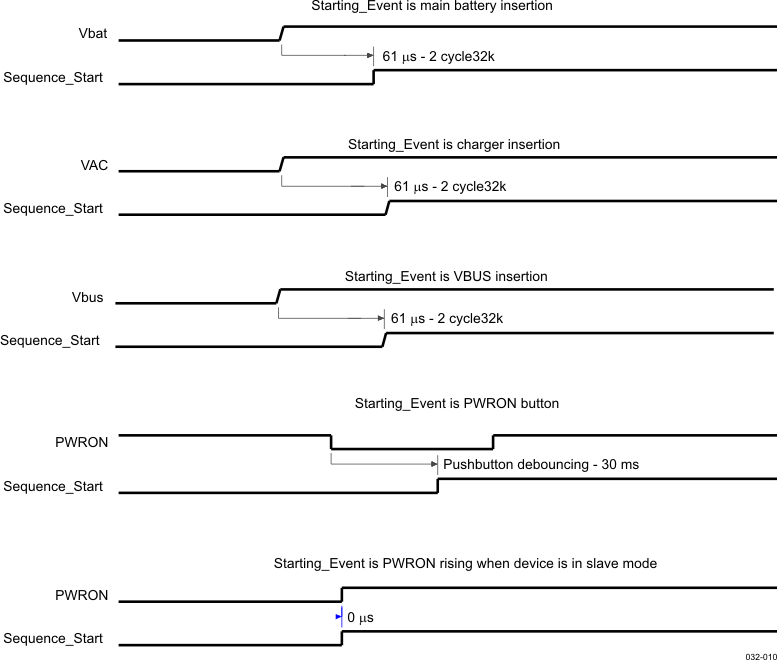 Figure 5-8 Timings Before Sequence Start
5.1.5.3.2 OMAP2 Power-On Sequence
Figure 5-9 shows the timing and control that must occur in Master_C027_Generic mode. Sequence_Start occurs according to the events shown in Figure 5-8.
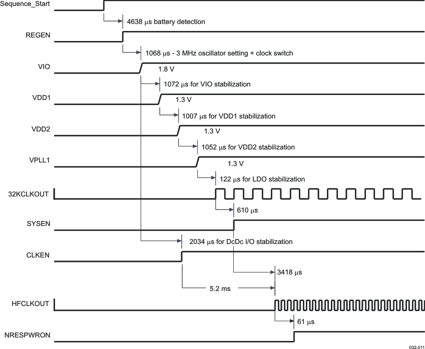 Figure 5-9 Timings—OMAP2 Power-On Sequence
5.1.5.3.3 OMAP3 Power-On Sequence
Figure 5-10 shows the timing and control that must occur in Master_C021_Generic mode. Sequence_Start occurs according to the events shown in Figure 5-8.
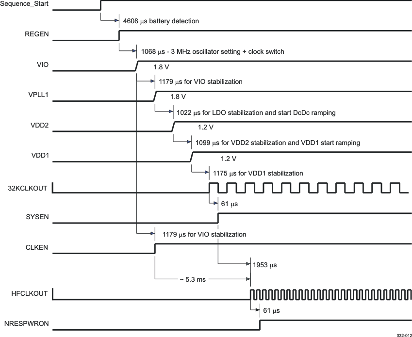 Figure 5-10 Timings—OMAP3 Power-On Sequence
5.1.5.3.4 Power On in Slave_C021_Generic Mode
Figure 5-11 describes the timing and control that must occur in the Slave_C021_Generic mode. Sequence_Start is a symbolic internal signal to ease the description of the power sequences and occurs according to the different events detailed in Figure 5-8.
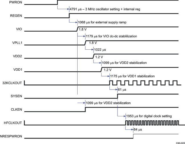 Figure 5-11 Timings—Power On in Slave_C021_Generic Model
5.1.5.4 Power-Off Sequence
This section describes the signal behavior required to power down the system.
5.1.5.4.1 Power-Off Sequence in Master Modes
Figure 5-12 shows the timing and control that occur during the power-off sequence in master modes.
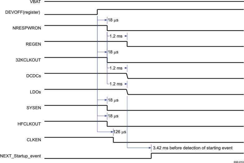
If the value of the HF clock is not 19.2 MHz (with the values of the CFG_BOOT HFCLK_FREQ bit field set accordingly), the delay between DEVOFF and NRESPWRON/CLK32KOUT/SYSEN/HFCLKOUT is divided by two (approximately 9 μs). This is caused by the internal frequency used by power STM switching from 3 to 1.5 MHz if the HF clock value is 19.2 MHz.
The DEVOFF event is PWRON falling edge in slave mode and DEVOFF internal register write in master mode.
5.2 Real-Time Clock and Embedded Power Controller
The TPS65950 device contains an RTC to provide clock and timekeeping functions and an EPC to provide battery supervision and control.
5.2.1 RTC
The RTC provides the following basic functions:
- Time information (seconds/minutes/hours) directly in binary-coded decimal (BCD) code
- Calendar information (day/month/year/day of the week) directly in BCD code
- Interrupt generation periodically (1 second/1 minute/1 hour/1 day) or at a precise time (alarm function)
- 32-kHz oscillator drift compensation and time correction
- Alarm-triggered system wake-up event
5.2.1.1 Backup Battery
The TPS65950 implements a backup mode in which a backup battery can keep the RTC running to maintain clock and time information even if the main supply is not present. If the backup battery is rechargeable, the device also provides a backup battery charger so it can be recharged when the main battery supply is present.
The backup domain powers the following:
- Internal 32.768-kHz crystal oscillator
- RTC
- Eight GP storage registers
- Backup domain low-power regulator (VBRTC)
5.2.2 EPC
The EPC provides five system states for optimal power use by the system, as listed in Table 5-27.
Table 5-27 System States
| System State | Description |
|---|---|
| NO SUPPLY | The system is not powered by any battery. |
| BACKUP | The system is powered only with the backup battery and maintains only the VBRTC supply. |
| WAIT-ON | The system is powered by the main battery and maintains only the VRRTC supply. It can accept switch-on requests. |
| ACTIVE | The system is powered by the main battery; all supplies can be enabled with full current capability. |
| SLEEP | The main battery powers the system; selected supplies are enabled, but in low consumption mode. |
Three categories of events can trigger state transitions:
- Hardware events: Supply/battery insertion, wake-up requests, USB plug, and RTC alarm
- Software events: Switch-off commands, switch-on commands, and sleep-on commands
- Monitoring events: Supply/battery level check, main battery removal, main battery fail, and thermal shutdown
5.3 Audio/Voice Module
The audio codec in the device includes five DACs and two ADCs to provide multiple voice channels and stereo downlink channels that can support all standard audio sample rates through I2S/TDM format interfaces. The audio output stages on the device include stereo headset amplifiers, two integrated class-D amplifiers providing stereo differential outputs, predrivers for line outputs, and an earpiece amplifier. The input audio stages include three differential microphone inputs, stereo line inputs, and interface for digital micrphones. Automatic and programmable gain control is available with all necessary digital filtering, side-tone functions, and pop-noise reduction.
Figure 5-13 is a block diagram of the audio/voice module.
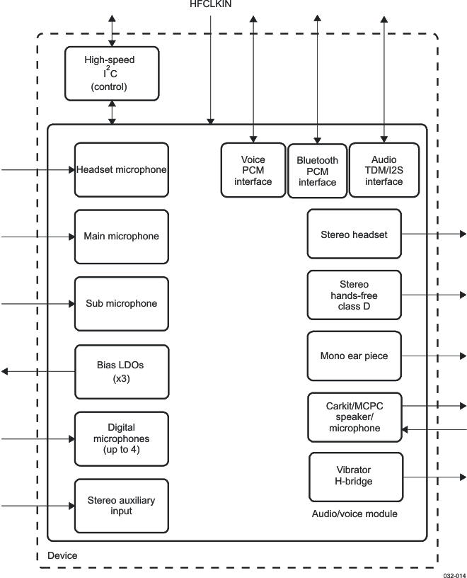 Figure 5-13 Audio/Voice Module Block Diagram
5.3.1 Audio/Voice Downlink (RX) Module
The audio/voice module includes the following output stages:
- Mono/stereo single-ended headset amplifier
- Stereo differential integrated class-D 8-Ω hands-free amplifiers
- Predriver output signals for external class-D amplifiers (single-ended)
- Mono differential earpiece amplifier
- Vibrator H-bridge
5.3.1.1 Earphone Output
5.3.1.1.1 Earphone Output Characteristics
Analog signals from the audio and/or voice interface are fed to the earphone amplifier. This amplifier, with different gains, provides a full differential signal on terminals EARP and EARM. Figure 5-14 shows the earphone amplifier. Table 5-28 lists the output characterstics of the earphone amplifier.
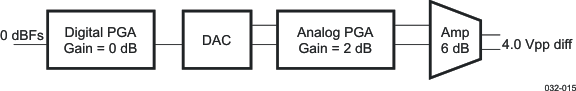 Figure 5-14 Earphone Amplifier
Table 5-28 Earphone Amplifier Output Characteristics
| Parameter | Test Conditions | Min | Typ | Max | Unit |
|---|---|---|---|---|---|
| Differential load impedance | 26 | 32 | Ω | ||
| 100 | 100 | pF | |||
| Gain range (2) | Audio path | –86 | 36 | dB | |
| Voice path | –60 | 36 | |||
| Absolute gain error | –1 | 1 | dB | ||
| Maximum output power | At 1.4 Vrms differential output voltage Load impedance = 32 Ω |
61.25 | mW | ||
| Peak-to-peak differential output voltage (0 dBFs) | Default gain (1) | 4.0 | VPP | ||
| Total harmonic distortion | At 0 dBFs | –65 | –60 | dB | |
| Default gain (1) | At –6 dBFs | –70 | –65 | ||
| Load impedance = 32 Ω | At –20 dBFs | –60 | |||
| At –60 dBFs | –30 | ||||
| Idle channel noise (20 Hz to 20 kHz, A-weighted) |
Gain = 0 dB Load = 32 Ω |
–90 | –85 | dBFs | |
| Output PSRR (for all gains) | 20 Hz to 4 kHz | 90 | dB | ||
| 20 Hz to 20 kHz | 70 |
Voice digital filter = –36 to 12 dB (1-dB steps)
ARXPGA (volume control) = –24 to 12 dB (2-dB steps)
Output driver = 0, 6, 12 dB
5.3.1.1.2 External Components and Application Schematic
Figure 5-15 is a simplified schematic of the earphone speaker.
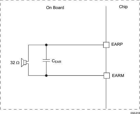 Figure 5-15 Earphone Speaker
NOTE
For the component values, see Table 5-92.
5.3.1.2 8-Ω Stereo Hands-Free
The digital signal from the audio and/or voice interface is fed to two class-D amplifiers. These 8-Ω speaker amplifiers provide a stereo differential signal on terminal pairs (IHF.RIGHT.P, IHF.RIGHT.M and IHF.LEFT.P, IHF.LEFT.M).
5.3.1.2.1 8-Ω Stereo Hands-Free Output Characteristics
Figure 5-16 shows the 8-Ω stereo hands-free amplifier. Table 5-29 lists the output characteristics of the 8-Ω stereo hands-free amplifier.
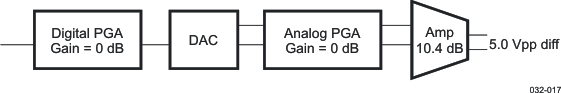 Figure 5-16 8-Ω Stereo Hands-Free Amplifiers
Table 5-29 8-Ω Stereo Hands-Free Output Characteristics
| Parameter | Test Conditions | Min | Typ | Max | Unit |
|---|---|---|---|---|---|
| VBAT voltage | 3.0 | 3.6 | 4.6 | V | |
| Load impedance | 6 | 8 | Ω | ||
| Gain range(1) | Audio path | –75.6 | 34.4 | dB | |
| Voice path | –49.6 | 34.4 | |||
| Absolute gain error | –1 | 1 | dB | ||
| Maximum output power (load impedance = 8 Ω) | VBAT > 3.6 V | 400 | mW | ||
| VBAT > 4.0 V | 700 | ||||
| Peak-to-peak differential output voltage | VBAT > 3.6 V (0 dBFs) | 5.0 | VPP | ||
| VBAT > 4.0 V (2 dBFs) | 6.25 | ||||
| Total harmonic distortion (load impedance = 8 Ω, gain setting = 0 dB) (VBAT > 3.6 V) |
At 0 dBFs | –60 | –40 | dBFs | |
| At –10 dBFs | –60 | ||||
| At –20 dBFs | –45 | ||||
| At –60 dBFs | –20 | ||||
| Total harmonic distortion (load impedance = 8 Ω, (VBAT > 4.2 V) | 2 dBFs | –60 | –40 | dB | |
| Idle channel noise (20 Hz to 20 kHz) | 0 dB gain | –88 | dBFs | ||
| PSRR (input signal 1 kHz sine, 300 mVPP GSM ripple at 217 Hz with 10-μs rise/fall times, at 12.5% duty cycle) | From VBAT | 75 | 80 | dB | |
| Efficiency | Power on load = 400 mW Load impedance = 8 Ω |
70% | |||
| Power dissipation | Power on load = 400 mW Load impedance = 8 Ω |
175 | mW | ||
| Idle current consumption on VBAT | Without input signal | 6 | mA | ||
| Clock frequency for the ramp generation | 384 | 426.6 | kHz | ||
| IDDQ current | At 25°C | 0.6 | μA |
Voice digital filter = –36 to 12 dB (1-dB steps)
ARXPGA (volume control) = –24 to 12 dB (2-dB steps)
Output driver = 10.4 dB
5.3.1.2.1.1 Short-Circuit Protection
There is short-circuit protection for hands-free amplifiers to limit power dissipation to 1.2 W. The short-circuit protection can be disabled by register. If a short circuit is detected, the short-circuit detection block switches off the hands-free speaker output stages. A software restart is required to restart the class-D amplifier.
5.3.1.2.2 External Components and Application Schematic
Figure 5-17 is a simplified schematic of the 8-Ω stereo hands-free.
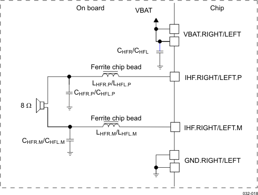 Figure 5-17 8-Ω Stereo Hands-Free
NOTE
For the component values, see Table 5-92.
For ferrite bead, choose one with high impedance at high frequencies, but with very low impedance at low frequencies. For example, MPZ1608S221A (recommended), N2012ZPS121, or MDP BKP1608HS271.
5.3.1.3 Headset
The analog signal from the audio and/or voice interface is fed to two single-ended headset amplifiers.
There are two configurations:
- Stereo single-ended mode: Left and right headset amplifiers with different gains (–6, 0, 6 dB) provide the stereo signal on the HSOL and HSOR terminals. A pseudo-ground is provided on the VMID terminal to eliminate external capacitors.
- Stereo single-ended mode ac-coupled: Left and right headset amplifiers with different gains (–6, 0, 6 dB) provide the stereo signal on the HSOL and HSOR terminals. The external capacitor is required to eliminate the dc component of the signal.
5.3.1.3.1 Headset Output Characteristics
Figure 5-18 shows the headset amplifier. Table 5-30 lists the output characteristics of the headset amplifier.
 Figure 5-18 Headset Amplifier
Table 5-30 Headset Output Characteristics
| Parameter | Test Conditions | Min | Typ | Max | Unit |
|---|---|---|---|---|---|
| Load impedance | 14 | 16 | Ω | ||
| 100 | 100 | pF | |||
| Gain range (2) | Audio path | –92 | 30 | dB | |
| Voice path | –66 | 30 | |||
| Absolute gain error | –1 | 1 | dB | ||
| Maximum output power | At 0.53 Vrms differential output voltage Load impedance = 16 Ω |
17.56 | mW | ||
| Peak-to-peak output voltage (0 dBFs) | Default gain (1) | 1.5 | VPP | ||
| Single-Ended Mode ac-Coupled | |||||
| Total harmonic distortion | At 0 dBFs | –80 | –75 | dB | |
| Default gain (1) | At –6 dBFs | –74 | –69 | ||
| Load = 16 Ω | At –20 dBFs | –70 | –65 | ||
| At –60 dBFs | –30 | –25 | |||
| Idle channel noise (20 Hz to 20 kHz, A-weighted) |
Default gain (1)
Load = 16 Ω |
–90 | –85 | dB | |
| SNR (A-weighted over 20-kHz bandwidth) | At 0 dBFs | 82 | 86 | dB | |
| Output PSRR (for all gains) | 20 Hz to 4 kHz | 90 | dB | ||
| 20 Hz to 20 kHz | 70 | ||||
| Crosstalk between right and left channels | –60 | dB | |||
| Single-Ended Mode (Pseudo-Ground Provided on HSOVMID) | |||||
| Total harmonic distortion | At 0 dBFs | –75 | –70 | dB | |
| Default gain (1) | At –6 dBFs | –74 | –69 | ||
| Load = 16 Ω | At –20 dBFs | –70 | –65 | ||
| At –60 dBFs | –30 | –25 | |||
| Idle channel noise (20 Hz to 20 kHz, A-weighted) |
Default gain (1)
Load = 16 Ω |
–90 | –85 | dB | |
| Output PSRR (for all gains) | 20 Hz to 4 kHz | 85 | dB | ||
| 20 Hz to 20 kHz | 65 | ||||
Voice digital filter = –36 to 12 dB (1-dB steps)
ARXPGA (volume control) = –24 to 12 dB (2-dB steps)
Output driver = –6, 0, 6 dB
5.3.1.3.2 External Components and Application Schematic
Figure 5-19 is a schematic of a headset 4-wire stereo jack without an external FET. Table 5-31 lists the output characteristics of this configuration.
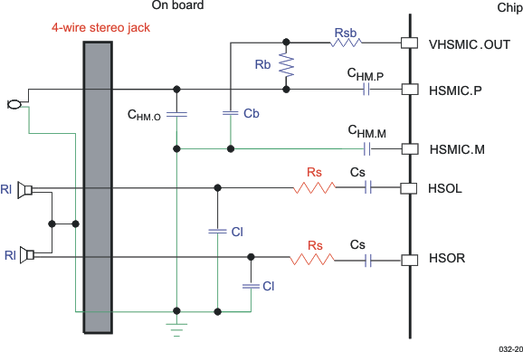 Figure 5-19 Headset 4-Wire Stereo Jack Without an External FET
Table 5-31 Output Characteristics of a Headset 4-Wire Stereo Jack Without an External FET
| Parameter | Test Conditions | Min | Typ | Max | Unit | |
|---|---|---|---|---|---|---|
| Rsb | Cb < 200 pF | 0 | Ω | |||
| Cb = 100 nF | 300 | |||||
| Cb = 1 μF | 500 | |||||
| Rb + Rsb | 2.2 | 2.7 | kΩ | |||
| Cs The input capacitors and output resistors form a high-pass filter (HPF) with the corner frequency = 1/(2πRout/Cs) |
22 | 47 | μF | |||
| RL | CL | |||||
| Rs required to ensure | 16 to 32 Ω | <100 pF | 0 | Ω | ||
| HS amplifier stability | 16 to 32 Ω | 1 nF | 4 | |||
| 16 Ω | 2 nF | 8 | ||||
| 24 Ω | 12 | |||||
| 32 Ω | 18 | |||||
| 16 Ω | 3 nF | 12 | ||||
| 24 Ω | 20 | |||||
| 32 Ω | 24 | |||||
| 16 Ω | 4 nF | 16 | ||||
| 24 Ω | 24 | |||||
| 32 Ω | 32 | |||||
| 16 Ω | 5 nF | 20 | ||||
| 24 Ω | 28 | |||||
| 32 Ω | 36 | |||||
NOTE
For other component values, see Table 5-92.
Table 5-32 is a schematic of a headset 4-wire stereo jack with an external FET. Table 5-32 lists the output characteristics of this configuration.
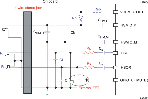 Figure 5-20 Headset 4-Wire Stereo Jack With an External FET
Table 5-32 Output Characteristics of a Headset 4-Wire Stereo Jack With an External FET
| Parameter | Test Conditions | Min | Typ | Max | Unit | |
|---|---|---|---|---|---|---|
| Rsb | Cb < 200 pF | 0 | Ω | |||
| Cb = 100 nF | 300 | |||||
| Cb = 1 μF | 500 | |||||
| Rb + Rsb | 2.2 | 2.7 | kΩ | |||
| Cs The input capacitors and output resistors form a HPF with the corner frequency = 1/(2πRout/Cs) |
22 | 47 | μF | |||
| RL | CL | |||||
| Rs required to ensure HS amplifier stability and no distortion caused by the parasitic diode of the external FET | 16 Ω | <2 nF | 10 | Ω | ||
| 24 Ω | 15 | |||||
| 32 Ω | 20 | |||||
| 16 Ω | 3 nF | 12 | ||||
| 24 Ω | 20 | |||||
| 32 Ω | 24 | |||||
| 16 Ω | 4 nF | 16 | ||||
| 24 Ω | 24 | |||||
| 32 Ω | 32 | |||||
| 16 Ω | 5 nF | 20 | ||||
| 24 Ω | 28 | |||||
| 32 Ω | 36 | |||||
NOTE
For other component values, see Table 5-92.
Figure 5-21 is a schematic of a headset 5-wire stereo jack. Table 5-33 lists the output characteristics of this configuration.
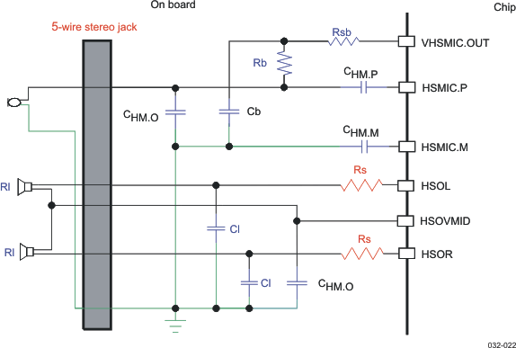 Figure 5-21 Headset 5-Wire Stereo Jack
Table 5-33 Output Characteristics of a Headset 5-Wire Stereo Jack
| Parameter | Test Conditions | Min | Typ | Max | Unit | |
|---|---|---|---|---|---|---|
| Rsb | Cb < 200 pF | 0 | Ω | |||
| Cb = 100 nF | 300 | |||||
| Cb = 1 μF | 500 | |||||
| Rb + Rsb | 2.2 | 2.7 | kΩ | |||
| RL | CL | |||||
| Rs required to ensure HS amplifier stability | 16 to 32 Ω | <100 pF | 0 | Ω | ||
| 16 to 32 Ω | 1 nF | 4 | ||||
| 16 Ω | 2 nF | 8 | ||||
| 24 Ω | 12 | |||||
| 32 Ω | 18 | |||||
| 16 Ω | 3 nF | 12 | ||||
| 24 Ω | 20 | |||||
| 32 Ω | 24 | |||||
| 16 Ω | 4 nF | 16 | ||||
| 24 Ω | 24 | |||||
| 32 Ω | 32 | |||||
| 16 Ω | 5 nF | 20 | ||||
| 24 Ω | 28 | |||||
| 32 Ω | 36 | |||||
NOTE
For other component values, see Table 5-92.
Figure 5-22 is a schematic of a headset 4-wire stereo jack optimized.
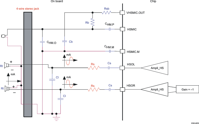 Figure 5-22 Headset 4-Wire Stereo Jack Optimized
NOTE
For other component values, see Table 5-92.
5.3.1.4 Headset Pop-Noise Attenuation
Pop noise occurs when the audio output amplifier is switched on. Although the speaker is ac-coupled through an external capacitor, the sharp rise time given by the activation of the amplifier causes a large spike to propagate to the speakers. Pop attenuation is achieved through a precharge and discharge of the external coupling capacitor.
The antipop system using an internal current generator controlling the ramp of charge or discharge is implemented for the headset output. The pop-noise effect can be dramatically reduced by an external FET controlled by a 1.8-V output signal (MUTE pin).
Figure 5-23 is a diagram of headset pop noise. Table 5-34 lists the characteristics of headset pop noise.
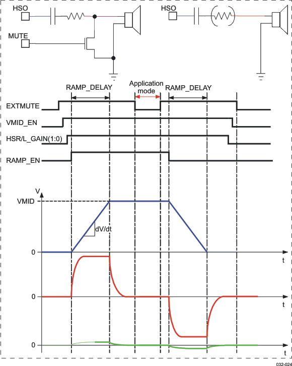 Figure 5-23 Headset Pop-Noise Cancellation Diagram
Table 5-34 Headset Pop-Noise Characteristics
| Parameter | Test Conditions | Min | Typ | Max | Unit |
|---|---|---|---|---|---|
| dv/dt | Ramp of charge or discharge | 170 | V/s | ||
| Pop-noise (A-weighted) | ac-coupling capacitor = 47 μF Serial resistor = 33 Ω External FET: Rdson = 0.12 Ω |
1 | mV |
5.3.1.5 Predriver for External Class-D Amplifier
Two predriver amplifiers provide a stereo signal on the PreD.LEFT and PreD.RIGHT terminals to drive an external class-D amplifier. These terminals are available if a stereo, single-ended, ac-coupled headset is used.
5.3.1.5.1 Predriver Output Characteristics
Table 5-35 lists the output characteristics of the predriver.
Table 5-35 Predriver Output Characteristics
| Parameter | Test Conditions | Min | Typ | Max | Unit |
|---|---|---|---|---|---|
| Load impedance | 10 | kΩ | |||
| 50 | pF | ||||
| Gain range (2) | Audio path | –92 | 30 | dB | |
| Voice path | –66 | 30 | |||
| Absolute gain error | –1 | 1 | dB | ||
| Peak-to-peak output voltage (0 dBFs) | Default gain (1) | 1.5 | VPP | ||
| Total harmonic distortion | At 0 dBFs | –80 | –75 | dB | |
| Default gain (1) | At –6 dBFs | –74 | –69 | ||
| Load > 10 kΩ // 50 pF | At –20 dBFs | –70 | –65 | ||
| At –60 dBFs | –30 | –25 | |||
| Idle channel noise (20 Hz to 20 kHz, A-weighted) | Default gain (1)
Load = 10 Ω |
–90 | –85 | dB | |
| SNR (A-weighted over 20-kHz bandwidth) | At 0 dBFs | 83 | 88 | dB | |
| Default gain(1) | At –60 dBFS | 30 | |||
| Output PSRR (for all gains) | 20 Hz to 4 kHz | 90 | dB | ||
| 20 Hz to 20 kHz | 70 |
Voice digital filter = –36 to 12 dB (1-dB steps)
ARXPGA (volume control) = –24 to 12 dB (2-dB steps)
Output driver = –6, 0, 6 dB
5.3.1.5.2 External Components and Application Schematic
Figure 5-24 is a simplified schematic of the external class-D predriver.
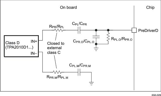 Figure 5-24 Predriver for External Class D
In Figure 5-24, input resistor (RPR or RPL) sets the gain of the external class D. For TPS2010D1, the gain is defined according to the following equation:
Gain (V/V) = 2*150*103/(RPR or RPL)
RPR or RPL > 15 kΩ
NOTE
For other component values, see Table 5-92.
5.3.1.6 Vibrator H-Bridge
A digital signal from the pulse width modulated generator is fed to the vibrator H-bridge driver. The vibrator H-bridge is a differential driver that drives vibrator motors. The differential output allows dual rotation directions.
5.3.1.6.1 Vibrator H-Bridge Output Characteristics
Table 5-36 lists the output characteristics of the vibrator H-bridge.
Table 5-36 Vibrator H-Bridge Output Characteristics
| Parameter | Test Conditions | Min | Typ | Max | Unit |
|---|---|---|---|---|---|
| VBAT voltage | 2.8 | 3.6 | 4.8 | V | |
| Differential output swing (16-Ω load) | VBAT = 2.8 V | 3.6 | VPP | ||
| VBAT = 3.5 V | 4.3 | ||||
| Output resistance (summed for both sides) | 8 | Ω | |||
| Load capacitance | 100 | pF | |||
| Load resistance | 8 | 16 | 60 | Ω | |
| Load inductance | 30 | 300 | μH | ||
| Total harmonic distortion | 10% | ||||
| Operating frequency | 20 | 10k | Hz |
5.3.1.6.2 External Components and Application Schematic
Figure 5-25 is a simplified schematic of the vibrator H-bridge.
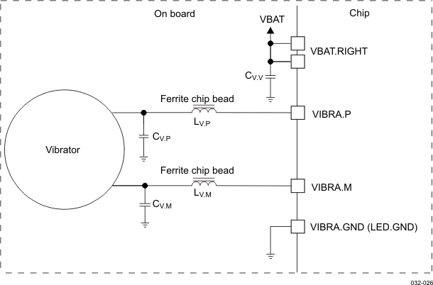 Figure 5-25 Vibrator H-Bridge
NOTE
For other component values, see Table 5-92.
Example of ferrite: BLM 18BD221SN1.
5.3.1.7 Carkit Output
The USB-CEA carkit uses the DP/DM pad to output audio signals (see the CEA-936A: Mini-USB Analog Carkit Interface Specification).
The MCPC carkit uses the RXAF analog pad to output audio signals.
Figure 5-26 shows the carkit output downlink full path characteristics for audio and USB.
 Figure 5-26 Carkit Output Downlink Path Characteristics
Table 5-37 lists the electrical characteristics of the MCPC and USB-CEA carkit audio.
Table 5-37 MCPC and USB-CEA Carkit Audio Downlink Electrical Characteristics
| Parameter | Conditions | Min | Typ | Max | Unit |
|---|---|---|---|---|---|
| Output load | USB-CEA (DP/DM) | 20 | kΩ | ||
| MCPC (RXAF) | 5 | ||||
| Gain range(2) | Audio path | –92 | 30 | dB | |
| Voice path | –66 | 30 | |||
| Absolute gain error | At 1 kHz | –1 | 1 | dB | |
| Peak-to-peak differential output voltage (0 dBFs) | Gain = 0 dB | 1.5 | VPP | ||
| Total harmonic distortion | At 0 dBFs | –80 | –75 | dB | |
| At –6 dBFs | –74 | –69 | |||
| At –20 dBFs | –70 | –65 | |||
| At –60 dBFs | –30 | –25 | |||
| THD+N (20 Hz to 20 kHz, A-weighted) | At 0 dBFs | 60 | dB | ||
| Idle channel noise (20 Hz to 20 kHz, A-weighted), default gain setting(1) | USB-CEA | –77 | dBFs | ||
| MCPC | –80 | –77 | |||
| Output PSRR | 20 Hz to 20 kHz | 60 | dB | ||
| Supply voltage (VINTANA1) | 1.5 | V | |||
| Common mode output voltage for USB-CEA | 1.3 | 1.35 | 1.4 | V | |
| Isolation between D+/D– during audio mode (20 Hz to 20 kHz) | 60 | dB | |||
| Crosstalk between right and left channels | USB-CEA stereo | –90 | dB | ||
| Crosstalk RX/TX (1 VPP output) | USB-CEA mono/stereo | –60 | dB | ||
| MCPC | –65 | ||||
| Signal noise ratio (20 Hz to 20 kHz, A-weighted) | At 0 dBFs | 60 | dB | ||
| Phone speaker amplifier output impedance at 1 kHz | USB-CEA (DP/DM) | 200 | Ω | ||
| MCPC (RXAF) | 200 |
Voice digital filter = –36 to 12 dB (1-dB steps);
ARXPGA (volume control) = –24 to 12 dB (2-dB steps);
Output driver (USB-CEA and MCPC) = –1 dB
5.3.1.8 Digital Audio Filter Module
Figure 5-27 shows the digital audio filter downlink full path characteristics of the audio interface.
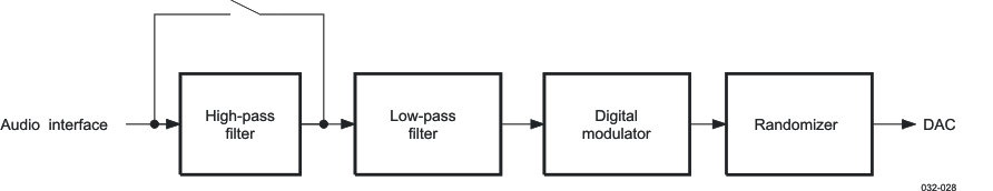 Figure 5-27 Digital Audio Filter Downlink Path Characteristics
The HPF can be bypassed.
Table 5-38 lists the audio filter frequency responses relative to reference gain at 1 kHz.
Table 5-38 Digital Audio Filter RX Electrical Characteristics
| Parameter | Conditions | Min | Typ | Max | Unit |
|---|---|---|---|---|---|
| Passband | 0.42 | FS | |||
| Passband ripple | 0 to 0.42FS(1) | –0.25 | 0.1 | 0.25 | dB |
| Stopband | 0.6 | FS | |||
| Stopband attenuation | F = 0.6FS(1) to 0.8FS(1) | 60 | 75 | dB | |
| Group delay | 15.8/FS(1) | μs | |||
| Linear phase | –1.4 | 1.4 | ° |
5.3.1.9 Digital Voice Filter Module
Figure 5-28 shows the digital voice filter downlink full path characteristics of the voice interface.
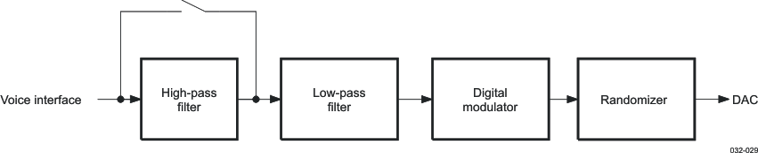 Figure 5-28 Digital Voice Filter Downlink Path Characteristics
The global HPF or only the third-order HPF can be bypassed (when the third-order HPF is skipped, the first-order HPF remains active).
5.3.1.9.1 Voice Downlink Filter (Sampling Frequency at 8 kHz)
Figure 5-29 shows the voice downlink frequency response with FS = 8 kHz. Table 5-39 lists the voice filter frequency responses relative to the reference gain at 1 kHz with FS = 8 kHz.
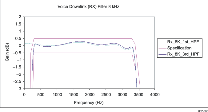 Figure 5-29 Voice Downlink Frequency Response With FS = 8 kHz
Table 5-39 Digital Voice Filter RX Electrical Characteristics With FS = 8 kHz
| Parameter | Test Conditions | Min | Typ | Max | Unit |
|---|---|---|---|---|---|
| Frequency response relative to reference gain at 1 kHz (first-order HPF) | 100 Hz | –20 | dB | ||
| 200 Hz | –8 | –0.5 | |||
| 300 to 3300 Hz | –0.5 | 0 | 0.5 | ||
| 3400 Hz | –1.5 | 0 | 0.1 | ||
| 4000 Hz | –17 | ||||
| 4600 Hz | –40 | ||||
| > 6000 Hz | –45 | ||||
| Pole when third-order HPF is disabled (first-order HPF) | 2.5 | Hz | |||
| Group delay | 0.5 | ms |
5.3.1.9.2 Voice Downlink Filter (Sampling Frequency at 16 kHz)
Figure 5-30 shows the voice downlink frequency response with FS = 16 kHz. Table 5-40 lists the voice filter frequency responses relative to the reference gain at 1 kHz with FS = 16 kHz.
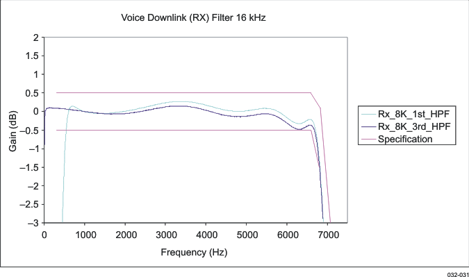 Figure 5-30 Voice Downlink Frequency Response With FS = 16 kHz
Table 5-40 Digital Voice Filter RX Electrical Characteristics With FS = 16 kHz
| Parameter | Test Conditions | Min | Typ | Max | Unit |
|---|---|---|---|---|---|
| Frequency response relative to reference gain at 1 kHz (first-order HPF) | 300 to 6600 Hz | –0.5 | 0 | 0.5 | dB |
| 6800 Hz | –1.5 | 0 | 0.1 | ||
| 8000 Hz | –17 | ||||
| 9200 Hz | –40 | ||||
| > 12000 Hz | –45 | ||||
| Pole when third-order HPF is disabled (first-order HPF) | 5 | Hz |
5.3.1.10 Boost Stage
The boost effect adds emphasis to low frequencies. It compensates for an HPF created by the capacitance resistor (CR) filter of the headset (in ac-coupling configuration).
There are four modes. Three effects are available, with slightly different frequency responses, and the fourth setting disables the boost effect:
- Boost effect 1
- Boost effect 2
- Boost effect 3
- Flat equalization: The boost effect is in bypass mode.
Table 5-41 and Table 5-42 list typical values according to frequency response versus input frequency and FS frequency.
Table 5-41 Boost Electrical Characteristics Versus FS Frequency (FS ≤ 22.05 kHz)
| Frequency (Hz) |
FS = 8 kHz | FS = 11.025 kHz | FS = 12 kHz | FS = 16 kHz | FS = 22.05 kHz | Unit | ||||||||||
|---|---|---|---|---|---|---|---|---|---|---|---|---|---|---|---|---|
| 1 | 2 | 3 | 1 | 2 | 3 | 1 | 2 | 3 | 1 | 2 | 3 | 1 | 2 | 3 | ||
| 10 | 4.51 | 5.13 | 5.62 | 5.10 | 5.51 | 5.80 | 5.22 | 5.58 | 5.83 | 5.54 | 5.77 | 5.92 | 5.76 | 5.89 | 5.97 | dB |
| 12 | 4.08 | 4.83 | 5.46 | 4.80 | 5.32 | 5.71 | 4.95 | 5.41 | 5.76 | 5.36 | 5.66 | 5.87 | 5.65 | 5.83 | 5.94 | |
| 15.2 | 3.43 | 4.32 | 5.18 | 4.28 | 4.97 | 5.54 | 4.47 | 5.11 | 5.61 | 5.03 | 5.47 | 5.79 | 5.45 | 5.71 | 5.90 | |
| 18.2 | 2.91 | 3.86 | 4.89 | 3.82 | 4.63 | 5.36 | 4.04 | 4.80 | 5.45 | 4.71 | 5.26 | 5.69 | 5.24 | 5.59 | 5.84 | |
| 20.5 | 2.56 | 3.53 | 4.65 | 3.49 | 4.37 | 5.21 | 3.72 | 4.56 | 5.32 | 4.45 | 5.09 | 5.60 | 5.06 | 5.49 | 5.79 | |
| 29.4 | 1.62 | 2.49 | 3.78 | 2.45 | 3.42 | 4.57 | 2.68 | 3.74 | 4.73 | 3.51 | 4.39 | 5.24 | 4.35 | 5.02 | 5.59 | |
| 39.7 | 1.05 | 1.71 | 2.93 | 1.67 | 2.55 | 3.84 | 1.88 | 2.80 | 4.06 | 2.66 | 3.63 | 4.72 | 3.67 | 4.45 | 5.27 | |
| 50.4 | 0.71 | 1.20 | 2.26 | 1.17 | 1.91 | 3.17 | 1.33 | 2.13 | 3.41 | 2.01 | 2.95 | 4.19 | 2.89 | 3.85 | 4.88 | |
| 60.3 | 0.51 | 0.92 | 1.79 | 0.89 | 1.49 | 2.65 | 1.00 | 1.68 | 2.89 | 1.57 | 2.43 | 3.72 | 2.39 | 3.35 | 4.52 | |
| 76.7 | 0.32 | 0.61 | 1.26 | 0.59 | 1.05 | 1.99 | 0.69 | 1.18 | 2.22 | 1.11 | 1.79 | 3.04 | 1.76 | 2.66 | 3.94 | |
| 97.5 | 0.20 | 0.39 | 0.87 | 0.38 | 0.70 | 1.43 | 0.44 | 0.79 | 1.62 | 0.75 | 1.27 | 2.36 | 1.24 | 2.00 | 3.28 | |
| 131.5 | 0.12 | 0.21 | 0.50 | 0.20 | 0.39 | 0.88 | 0.25 | 0.47 | 1.02 | 0.42 | 0.78 | 1.59 | 0.75 | 1.30 | 2.41 | |
| 157 | 0.08 | 0.15 | 0.36 | 0.15 | 0.28 | 0.65 | 0.17 | 0.33 | 0.75 | 0.31 | 0.57 | 1.22 | 0.55 | 0.99 | 1.93 | |
| 200 | 0.05 | 0.09 | 0.22 | 0.09 | 0.17 | 0.41 | 0.11 | 0.21 | 0.49 | 0.19 | 0.37 | 0.82 | 0.36 | 0.66 | 1.38 | |
| 240 | 0.03 | 0.06 | 0.15 | 0.06 | 0.12 | 0.29 | 0.07 | 0.14 | 0.35 | 0.14 | 0.26 | 0.60 | 0.25 | 0.48 | 1.04 | |
| 304 | 0.02 | 0.04 | 0.09 | 0.04 | 0.07 | 0.18 | 0.04 | 0.09 | 0.22 | 0.08 | 0.16 | 0.38 | 0.16 | 0.30 | 0.70 | |
| 463 | 0.00 | 0.01 | 0.03 | 0.01 | 0.03 | 0.07 | 0.02 | 0.04 | 0.09 | 0.03 | 0.07 | 0.17 | 0.07 | 0.13 | 0.32 | |
| 704 | 0.00 | 0.00 | 0.01 | 0.00 | 0.01 | 0.03 | 0.01 | 0.01 | 0.03 | 0.01 | 0.03 | 0.07 | 0.03 | 0.06 | 0.14 | |
| 1008 | 0.00 | 0.00 | 0.00 | 0.00 | 0.00 | 0.01 | 0.00 | 0.00 | 0.01 | 0.00 | 0.01 | 0.03 | 0.01 | 0.02 | 0.06 | |
| 1444 | 0.00 | 0.00 | 0.00 | 0.00 | 0.00 | 0.00 | 0.00 | 0.00 | 0.00 | 0.00 | 0.00 | 0.00 | 0.00 | 0.01 | 0.02 | |
| 2070 | 0.00 | 0.00 | 0.00 | 0.00 | 0.00 | 0.00 | 0.00 | 0.00 | 0.00 | 0.00 | 0.00 | 0.00 | 0.00 | 0.00 | 0.01 | |
| 3770 | 0.00 | 0.00 | 0.00 | 0.00 | 0.00 | 0.00 | 0.00 | 0.00 | 0.00 | 0.00 | 0.00 | 0.00 | 0.00 | 0.00 | 0.00 | |
Table 5-42 Boost Electrical Characteristics Versus FS Frequency (FS ≥ 24 kHz)
| Frequency (Hz) |
FS = 24 kHz | FS = 32 kHz | FS = 44.1 kHz | FS = 48 kHz | FS = 96 kHz | Unit | ||||||||||
|---|---|---|---|---|---|---|---|---|---|---|---|---|---|---|---|---|
| 1 | 2 | 3 | 1 | 2 | 3 | 1 | 2 | 3 | 1 | 2 | 3 | 1 | 2 | 3 | ||
| 10 | 5.79 | 5.90 | 5.97 | 5.89 | 5.89 | 5.99 | 5.95 | 5.98 | 6.04 | 5.96 | 5.99 | 6.01 | 5.71 | 5.83 | 5.90 | dB |
| 12 | 5.70 | 5.85 | 5.95 | 5.84 | 5.84 | 5.98 | 5.92 | 5.97 | 6.03 | 5.94 | 5.98 | 6.00 | 5.54 | 5.68 | 5.81 | |
| 15.2 | 5.53 | 5.76 | 5.91 | 5.73 | 5.73 | 5.96 | 5.87 | 5.94 | 6.02 | 5.89 | 5.95 | 5.99 | 5.40 | 5.57 | 5.73 | |
| 18.2 | 5.35 | 5.65 | 5.87 | 5.62 | 5.62 | 5.93 | 5.80 | 5.90 | 6.00 | 5.83 | 5.93 | 5.98 | 5.28 | 5.48 | 5.68 | |
| 20.5 | 5.19 | 5.56 | 5.83 | 5.52 | 5.52 | 5.91 | 5.74 | 5.87 | 5.99 | 5.78 | 5.90 | 5.97 | 5.19 | 5.42 | 5.64 | |
| 29.4 | 4.55 | 5.18 | 5.64 | 5.10 | 5.07 | 5.79 | 5.51 | 5.75 | 5.94 | 5.57 | 5.79 | 5.92 | 4.87 | 5.18 | 5.48 | |
| 39.7 | 3.81 | 4.62 | 5.37 | 4.52 | 4.52 | 5.64 | 5.12 | 5.53 | 5.85 | 5.26 | 5.59 | 5.84 | 4.47 | 4.91 | 5.30 | |
| 50.4 | 3.14 | 4.06 | 5.02 | 3.94 | 3.95 | 5.43 | 4.69 | 5.27 | 5.72 | 4.88 | 5.37 | 5.73 | 4.08 | 4.63 | 5.11 | |
| 60.3 | 2.62 | 3.51 | 4.69 | 3.46 | 3.54 | 5.21 | 4.30 | 5.00 | 5.59 | 4.49 | 5.13 | 5.62 | 3.72 | 4.37 | 4.95 | |
| 76.7 | 1.97 | 2.90 | 4.15 | 2.76 | 2.76 | 4.78 | 3.68 | 4.52 | 5.34 | 3.91 | 4.70 | 5.40 | 3.18 | 3.92 | 4.67 | |
| 97.5 | 1.41 | 2.22 | 3.51 | 2.10 | 2.09 | 4.27 | 2.99 | 3.94 | 4.99 | 3.24 | 4.15 | 5.07 | 2.59 | 3.41 | 4.33 | |
| 131.5 | 0.88 | 1.49 | 2.65 | 1.40 | 1.40 | 3.49 | 2.15 | 3.10 | 4.35 | 2.38 | 3.35 | 4.51 | 1.86 | 2.69 | 3.75 | |
| 157 | 0.65 | 1.13 | 2.15 | 1.04 | 1.04 | 2.96 | 1.70 | 2.58 | 3.90 | 1.90 | 2.82 | 4.08 | 1.47 | 2.24 | 3.35 | |
| 200 | 0.41 | 0.76 | 1.55 | 0.70 | 0.70 | 2.28 | 1.19 | 1.93 | 3.23 | 1.35 | 2.15 | 3.44 | 1.03 | 1.68 | 2.77 | |
| 240 | 0.30 | 0.55 | 1.18 | 0.50 | 0.50 | 1.81 | 0.89 | 1.51 | 2.71 | 1.02 | 1.70 | 2.92 | 0.77 | 1.31 | 2.32 | |
| 304 | 0.18 | 0.35 | 0.80 | 0.33 | 0.32 | 1.27 | 0.58 | 1.04 | 2.05 | 0.68 | 1.19 | 2.24 | 0.51 | 0.90 | 1.75 | |
| 463 | 0.08 | 0.16 | 0.37 | 0.14 | 0.14 | 0.64 | 0.27 | 0.50 | 1.12 | 0.31 | 0.58 | 1.25 | 0.23 | 0.43 | 0.95 | |
| 704 | 0.03 | 0.06 | 0.16 | 0.06 | 0.06 | 0.29 | 0.12 | 0.23 | 0.56 | 0.14 | 0.27 | 0.62 | 0.10 | 0.20 | 0.46 | |
| 1008 | 0.01 | 0.03 | 0.07 | 0.03 | 0.02 | 0.14 | 0.06 | 0.11 | 0.30 | 0.06 | 0.13 | 0.31 | 0.05 | 0.10 | 0.23 | |
| 1444 | 0.00 | 0.01 | 0.03 | 0.01 | 0.01 | 0.06 | 0.03 | 0.05 | 0.16 | 0.03 | 0.06 | 0.15 | 0.02 | 0.05 | 0.11 | |
| 2070 | 0.00 | 0.00 | 0.01 | 0.00 | 0.00 | 0.02 | 0.01 | 0.02 | 0.09 | 0.01 | 0.03 | 0.07 | 0.01 | 0.02 | 0.05 | |
| 3770 | 0.00 | 0.00 | 0.00 | 0.00 | 0.00 | 0.00 | 0.00 | 0.00 | 0.04 | 0.00 | 0.00 | 0.01 | 0.00 | 0.00 | 0.01 | |
5.3.2 Audio/Voice Uplink (TX) Module
The voice uplink path includes two input amplification stages dedicated to ten analog input terminals:
- MIC_MAIN_P, MIC_MAIN_M (differential main handset input)
- MIC_SUB_P, MIC_SUB_M (differential sub handset input)
- HSMICP, HSMICM (differential headset input)
- AUXL (common terminal: single-ended auxiliary/FM radio left channel input)
- AUXR (common terminal: single-ended auxiliary/FM radio right channel input)
- CEA carkit and MCPC transmit audio (TXAF) microphone through DINP/DINM pins
For all cases, only two analog input amplifiers can be used, because two ADCs are available.
The voice uplink path also includes two pulse density modulated (PDM) interfaces for digital microphones. Two stereo digital microphone interfaces are available.
The left and right FM channels can be connected to any audio output stage (for example, earpiece, headset speakers, etc.) through a connection matrix.
5.3.2.1 Microphone Bias Module
Three bias generators provide an external voltage of 2.2 V to bias the analog microphones (MICBIAS1, MICBIAS2, and HSMICBIAS terminals). The typical output current is 1 mA for each analog bias microphone.
Two bias generators can provide an external voltage of 1.8 V to bias digital microphones (DIGMIC_0 and DIGMIC_1). The typical output current is 5 mA for each digital bias microphone.
NOTE
One bias generator can bias two digital microphones at the same time; in this case, the typical output current is 10 mA.
Figure 5-31 shows the multiplexing for the analog and digital microphones.
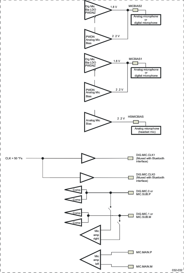 Figure 5-31 Analog and Digital Microphone Multiplexing
5.3.2.1.1 Analog Microphone Bias Module Characteristics
Table 5-43 lists the characteristics of the analog microphone bias module.
Table 5-43 Analog Microphone Bias Module Characteristics
| Parameter | Test Conditions | Min | Typ | Max | Unit |
|---|---|---|---|---|---|
| Bias voltage | 2.15 | 2.2 | 2.25 | V | |
| Load current | 1 | mA | |||
| Output noise | P-weighted 20 Hz to 6.6 kHz | 1.8 | μVRMS | ||
| External capacitor | 0 | 200 | pF | ||
| Internal resistance | 50 | 60 | 70 | kΩ |
NOTE
If the value of the external capacitor is greater than 200 pF, the analog microphone bias becomes unstable. To stabilize it, a serial resistor must be added.
Table 5-44 lists the characteristics of the analog microphone bias module with a bias resistor.
Table 5-44 Characteristics of Analog Microphone Bias Module With a Bias Resistor
| Parameter | Test Conditions | Min | Typ | Max | Unit |
|---|---|---|---|---|---|
| RSB | CB < 200 pF | 0 | Ω | ||
| CB = 100 pF | 300 | ||||
| CB = 1 μF | 500 | ||||
| RB + RSB | 2.2 to 2.7 | kΩ |
5.3.2.1.2 External Components and Application Schematic
Figure 5-32 and Figure 5-33 show the external components and application schematics for the analog microphone.
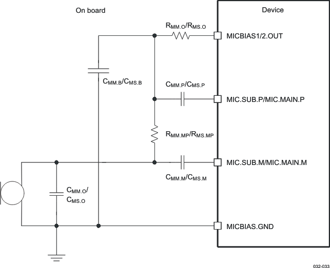 Figure 5-32 Analog Microphone Pseudodifferential
NOTE
For other component values, see Table 5-92.
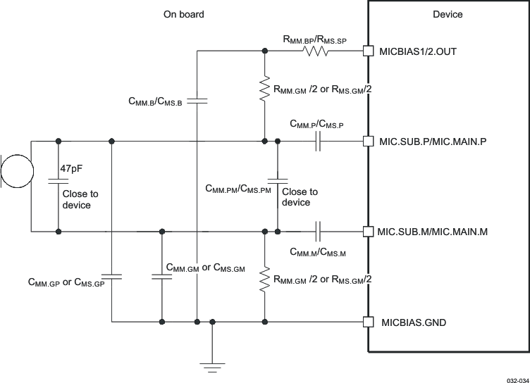 Figure 5-33 Analog Microphone Differential
NOTE
For other component values, see Table 5-92.
NOTE
To improve the rejection, it is highly recommended to ensure that MICBIAS_GND is as clean as possible. This ground must be shared with AGND of TPS65950 and must not share with AVSS4, which is the ground used by RX class-AB output stages.
In differential mode, adding a low-pass filter (made by RSB and CB) is highly recommended if coupling between RX output stages and the microphone is too high (and there is not enough attenuation by the echo cancellation algorithm). The coupling can come from:
- The internal TPS65950 coupling between MICBIAS.OUT voltage and RX output stages
- Coupling noise between MICBIAS.GND and AVSS4
In pseudodifferential mode, the dynamic resistance of the microphone improves the rejection versus MICBIAS.OUT:
PSRR = 20*log((RB + RDyn_mic)/RB)
5.3.2.1.3 Digital Microphone Bias Module Characteristics
Figure 5-34 is a block diagram of the digital microphone bias module.
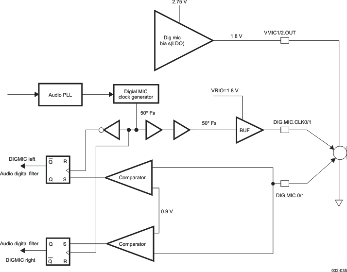 Figure 5-34 Digital Microphone Bias Module Block Diagram
Table 5-45 and Table 5-46 list the characteristics of the digital microphone bias module.
Table 5-45 Digital Microphone Bias Module Characteristics
| Parameter | Test Conditions | Min | Typ | Max | Unit |
|---|---|---|---|---|---|
| Bias voltage | 1.8 | V | |||
| Load current | 10 | mA | |||
| PSRR (from VBAT) | 20 Hz to 6.6 kHz | 60 | dB | ||
| External capacitor | 0.3 | 1 | 3.3 | μF | |
| ESR for capacitor | At 100 kHz | 0.02 | 0.6 | Ω |
Table 5-46 Digital Microphone Bias Module Characteristics (2)
| Parameter | Test Conditions | Min | Typ | Max | Unit |
|---|---|---|---|---|---|
| Comparator high threshold | 0.5*VDD_IO | 0.7*VDD_IO | |||
| Comparator low threshold | 0.3*VDD_IO | 0.5*VDD_IO | |||
| Startup time | 2 | μs | |||
| DIG.MIC.0 (tHOLD) from DIG.MIC.CLK0 edge | 4 | ns | |||
| DIG.MIC.1 (tHOLD) from DIG.MIC.CLK1 edge | 4 | ns |
Figure 5-35 is a timing diagram of the digital microphone bias module.
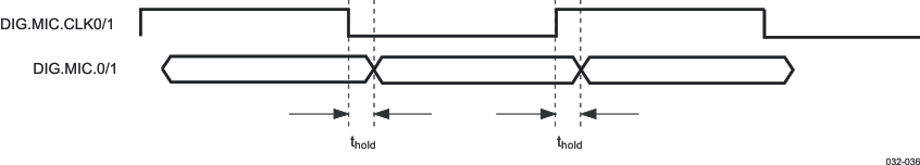 Figure 5-35 Digital Microphone Bias Module Timing Diagram
5.3.2.1.4 Silicon Microphone Characteristics
Based on silicon micro-electrical-mechanical system (MEMS) technology, the new microphone achieves the same acoustic and electrical properties as conventional microphones, but is more rugged and exhibits higher heat resistance. These properties offer designers greater flexibility and new opportunities to integrate microphones.
The silicon microphone is the integration of mechanical elements and electronics on a common silicon substrate through microfabrication technology.
The complementary metal oxide semiconductor (CMOS) MEMS microphone is more like an analog IC than a classic electric condenser microphone (ECM). It is powered as an IC with a direct connection to the power supply. The on-chip isolation between the power input and the rest of the system adds power supply rejection (PSR) to the component, making the CMOS MEMS microphone inherently more immune to power supply noise than an ECM and eliminating the need for additional filtering circuitry to keep the power supply line clean.
Figure 5-36 is a schematic of the silicon microphone module.
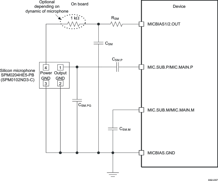 Figure 5-36 Silicon Microphone Module
Table 5-47 lists the characteristics of the silicon microphone module.
Table 5-47 Silicon Microphone Module Characteristics
| Parameter | Test Conditions | Min | Typ | Max | Unit |
|---|---|---|---|---|---|
| Bias voltage | 2.2 | V | |||
| Load current | 1 | mA | |||
| Output noise | P-weighted 20 Hz to 6.6 kHz | 1.8 | μVRMS |
NOTE
For other component values, see Table 5-92.
5.3.2.2 Stereo Differential Input
The stereo differential inputs (the MIC_MAIN_P and MIC_MAIN_M, and the MIC_SUB_P and MIC_SUB_M terminals) can be amplified by the microphone amplification stages. The amplification stage outputs are connected to the two ADC inputs.
5.3.2.3 Headset Differential Input
The headset differential inputs (the HSMICP and HSMICM terminals) can be amplified by the microphone amplification stage. The amplification stage outputs are connected to the ADC input.
5.3.2.4 FM Radio/Auxiliary Stereo Input
The auxiliary inputs AUXL/FML and AUXR/FMR can be used as the left and right stereo inputs, respectively, of the FM radio. In that case (because both input amplifiers are busy), the other input terminals are discarded and set to a high-impedance state. Both microphone amplification stages amplify the FM radio stereo signal. Both amplification stage outputs are connected to the ADC input. The left and right channel inputs of the FM radio can also be output through an audio output stage (mono output stage in case of mono input FM radio, stereo output stage in case of stereo input FM radio).
5.3.2.4.1 External Components
Figure 5-37 shows the external components of the auxiliary stereo input.
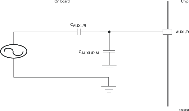 Figure 5-37 Audio Auxiliary Input
NOTE
For other component values, see Table 5-92.
5.3.2.5 PDM Interface for Digital Microphones
The PDM interface is used as digital microphone inputs; each microphone is directly connected to the TX filter decimator to extract the audio samples at the desired accuracy and sample rate. Each digital microphone is stereo (two paths). The digital microphone interface is DIG.MIC.CLK (clock input to the microphone) and DIG.MIC (PDM data output from the microphone). The appropriate frequency of DIG.MIC.CLK is generated by the audio PLL, and the ratio between DIG.MIC.CLK and the sample rate is 50 (see Figure 5-38). The PDM interface is available only when FS = 48 kHz.
The data signal output is a 3-state output from the microphone. When a falling-edge DIG.MIC.CLK is detected, DIG.MIC is actively driven. When a rising DIG.MIC.CLK is detected, DIG.MIC is high impedance. The latter DIG.MIC.CLK half-cycle is reserved for stereo operation (the second microphone receives DIG.MIC.CLK inverted).
The Σ-Δ converter in the digital microphones produces PDM.
Digital microphone characteristics:
- PDM clock rate 2.4 MHz
- Fourth-order Σ-Δ converter in the microphone component
Figure 5-38 is an example of PDM interface circuitry.
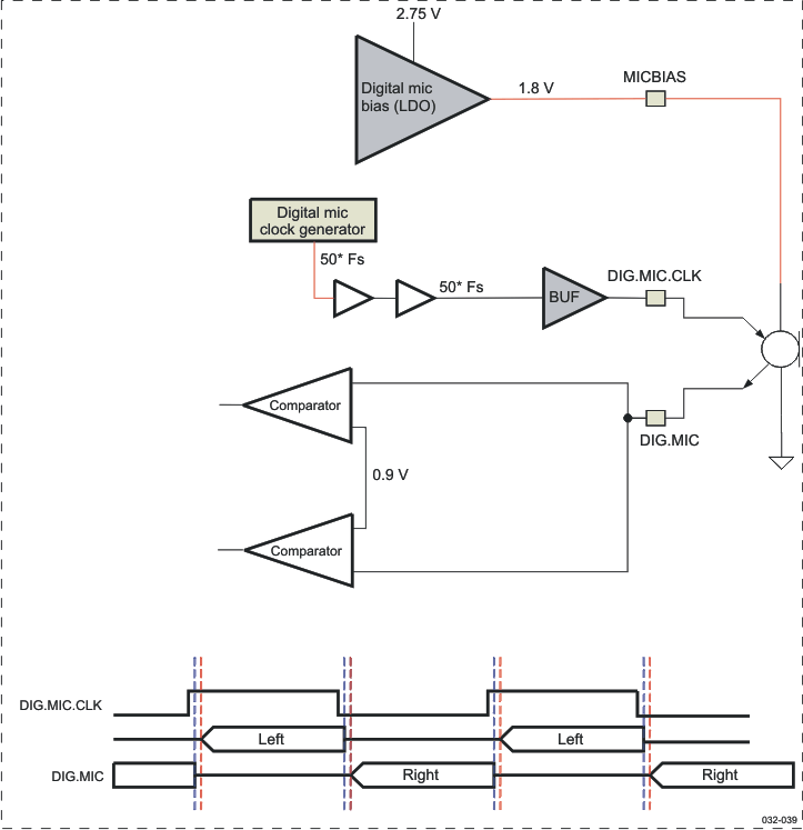 Figure 5-38 Example of PDM Interface Circuitry
5.3.2.6 Uplink Characteristics
Figure 5-39 shows the uplink amplifier. Table 5-48 lists the characteristics of the uplink amplifier.
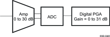 Figure 5-39 Uplink Amplifier
Table 5-48 Uplink Amplifier Characteristics
| Parameter | Test Conditions | Min | Typ | Max | Unit |
|---|---|---|---|---|---|
| Speech delay | Voice path | 0.5 | ms | ||
| Gain range(1) | 0 | 61 | dB | ||
| Absolute gain | 0 dBFs at 1.02 kHz | –1 | 1 | dB | |
| Peak-to-peak differential input voltage (0 dBFs) | For differential input 0 dB gain setting |
1.5 | VPP | ||
| Peak-to-peak single-ended input voltage (0 dBFs) | For single-ended input 0 dB gain setting |
1.5 | VPP | ||
| Input impedance(2) | 40k | 70k | Ω | ||
| Total harmonic distortion (sine wave at 1.02 kHz) | At –1 dBFs | –80 | –75 | dB | |
| At –6 dBFs | –74 | –69 | |||
| At –10 dBFs | –70 | –65 | |||
| At –20 dBFs | –60 | –55 | |||
| At –60 dBFs | –20 | –15 | |||
| Idle channel noise | 20 Hz to 20 kHz, A-weighted, gain = 0 dB | –85 | –78 | dBFs | |
| 16 kHz: < 20 Hz to 7 kHz, gain = 0 dB | –90 | ||||
| 8 kHz: P-weighted voice, gain = 18 dB | –87 | ||||
| 16 kHz: < 20 Hz to 7 kHz, gain = 18 dB | –82 | ||||
| Crosstalk A/D to D/A | Gain = 0 dB | –80 | dB | ||
| Crosstalk path between two microphones | –70 | dB | |||
| Intermodulation distortion | Two-tone method | –60 | dB |
5.3.2.7 Microphone Amplification Stage
Microphone amplification stages perform single-to-differential conversion for single-ended inputs. Two programmable gains from 0 to 30 dB can be set:
- Automatic level control for main microphone or submicrophone input. The gain step is 1 dB.
- Level control by register for line-in or carkit input, or headset microphone. The gain step is 6 dB.
The amplification stage outputs are connected to the ADC input (ADC left and right).
5.3.2.8 Carkit Input
The USB-CEA carkit uses the DP pad to input the audio signal.
The MCPC carkit uses the TXAF analog pad to input the audio signal.
Figure 5-40 shows the uplink carkit full path uplink characteristics for audio and USB.
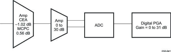 Figure 5-40 Carkit Input Uplink Path Characteristics
Table 5-49 lists the electrical characteristics of the MCPC and USB-CEA carkit audio.
Table 5-49 MCPC and USB-CEA Carkit Audio Uplink Electrical Characteristics
| Parameter | Test Conditions | Min | Typ | Max | Unit |
|---|---|---|---|---|---|
| Gain range (1) | –1 | 60 | dB | ||
| Absolute gain, 0 dBFs at 1.02 kHz (1)(2)(3) | USB-CEA default gain setting | –1.5 | 1.5 | dB | |
| MCPC default gain setting | –1.5 | 1.5 | |||
| Speech delay | Voice path | 0.5 | ms | ||
| Input common mode voltage (4) | USB-CEA | 1.3 | 1.9 | V | |
| Phone microphone amplifier input impedance at 1 kHz | USB-CEA | 8 | 120 | kΩ | |
| MCPC | 5 | 100 | |||
| Peak-to-peak single-ended input voltage (0 dBFs) | Default setting | 1.414 | VPP | ||
| Total harmonic distortion (sine wave at 1 kHz), default gain setting | At –1 dBFs | –74 | –60 | dB | |
| At –6 dBFs | |||||
| At –10 dBFs | |||||
| At –20 dBFs | |||||
| At –60 dBFs | |||||
| THD + N (20 Hz to 20 kHz, A-weighted) | At 0 dBFs | 60 | dB | ||
| Signal noise ratio (20 Hz to 20 kHz, A-weighted) | At 0 dBFs | 60 | dB | ||
| Idle channel noise (20 Hz to 20 kHz, A-weighted), default gain setting | USB-CEA | –77 | dBFs | ||
| MCPC | –80 | –77 | |||
| Output PSRR (20 Hz to 20 kHz, A-weighted) | USB-CEA | 50 | dB | ||
| MCPC | 35 |
5.3.2.9 Digital Audio Filter Module
Figure 5-41 shows the digital audio filter uplink full path characteristics for the audio interface.
 Figure 5-41 Digital Audio Filter Uplink Path Characteristics
The HPF can be bypassed. It is controlled by the MISC_SET_2 ATX_HPF_BYP bit, address 0x49.
Table 5-50 lists the audio filter frequency responses relative to reference gain at 1 kHz.
Table 5-50 Digital Audio Filter TX Electrical Characteristics
| Parameter | Test Conditions | Min | Typ | Max | Unit |
|---|---|---|---|---|---|
| Passband | 0.0005 | 0.42 | FS | ||
| Passband gain | In region 0.0005*FS to 0.42*FS(1) | –0.25 | 0.25 | dB | |
| Stopband | 0.6 | FS | |||
| Stopband attenuation | In region 0.6*FS to 1*FS(1) | 60 | dB | ||
| Group delay | 15.8/FS | μs |
5.3.2.10 Digital Voice Filter Module
Figure 5-42 shows the digital voice filter uplink full path characteristics of the voice interface.
 Figure 5-42 Digital Audio Filter Uplink Path Characteristics
The global HPF or only the third-order HPF can be bypassed (when the third-order HPF is skipped, the first-order HPF remains active). It is controlled by the MISC_SET_2 VTX_3RD_HPF_BYP bit, address 0x49, the for the third-order HPF, and by the VTX_HPF_BYP bit for the global HPF.
5.3.2.10.1 Voice Uplink Filter (Sampling Frequency at 8 kHz)
Figure 5-43 and Figure 5-44 show the voice uplink frequency response with a sampling frequency of 8 kHz.
 Figure 5-43 Voice Uplink Frequency Response With FS = 8 kHz (Frequency Range 0 to 600 Hz)
 Figure 5-44 Voice Uplink Frequency Response With FS = 8 kHz (Frequency Range 3000 to 3600 Hz)
Table 5-51 lists the voice filter frequency responses relative to reference gain at 1 kHz with FS = 8 kHz.
Table 5-51 Digital Voice Filter TX Electrical Characteristics With FS = 8 kHz
| Parameter | Test Conditions | Min | Typ | Max | Unit |
|---|---|---|---|---|---|
| Frequency response relative to reference gain at 1 kHz | 100 Hz | –20 | dB | ||
| 200 Hz | –8 | –0.5 | |||
| 300 to 3300 Hz | –0.5 | 0 | 0.5 | ||
| 3400 Hz | –1.5 | 0 | 0.1 | ||
| 4000 Hz | –17 | ||||
| 4600 Hz | –40 | ||||
| >6000 Hz | –45 | ||||
| Pole when HPF is disabled (first-order HPF) | 24 | Hz | |||
| Group delay | 0.5 | ms |
5.3.2.10.2 Voice Uplink Filter (Sampling Frequency at 16 kHz)
Figure 5-45 and Figure 5-46 show the voice uplink frequency response with a sampling frequency of 16 kHz.
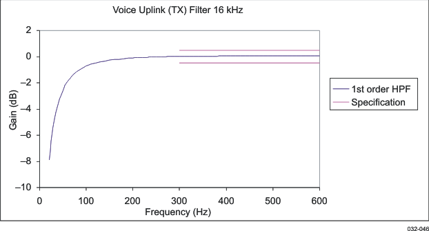 Figure 5-45 Voice Uplink Frequency Response With FS = 16 kHz (Frequency Range 0 to 600 Hz)
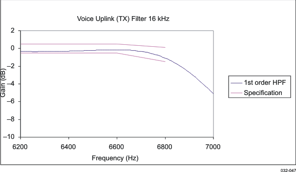 Figure 5-46 Voice Uplink Frequency Response With FS = 16 kHz (Frequency Range 6200 to 7000 Hz)
Table 5-52 lists the voice filter frequency responses relative to reference gain at 1 kHz with FS = 16 kHz.
Table 5-52 Digital Voice Filter TX Electrical Characteristics With FS = 16 kHz
| Parameter | Test Conditions | Min | Typ | Max | Unit |
|---|---|---|---|---|---|
| Frequency response relative to reference gain at 1 kHz (first-order HPF) | 300 to 6600 Hz | –0.5 | 0.5 | dB | |
| 6800 Hz | –1.5 | 0.1 | |||
| 8000 Hz | –0.5 | 0 | –17 | ||
| 9200 Hz | –1.5 | 0 | –40 | ||
| 12000 Hz | –45 | ||||
| Pole when third-order HPF is disabled (first-order HPF) | 47 | Hz |
5.4 USB HS 2.0 OTG Transceiver
The TPS65950 includes a USB OTG transceiver with CEA and MCPC carkit interfaces that support USB 480 Mbps HS, 12 Mbps full-speed (FS), and USB 1.5 Mbps low-speed (LS) through a 4-pin ULPI.
The carkit block ensures the interface between the phone and a carkit device. The TPS65950 USB supports CEA and MCPC carkit standards.
Figure 5-47 is a block diagram of the USB 2.0 physical layer (PHY).
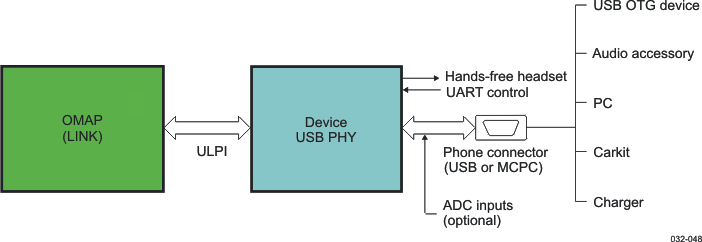 Figure 5-47 USB 2.0 PHY Overview
5.4.1 USB Features
The device has a USB OTG carkit transceiver that allows system implementation that complies with the following specifications:
- Universal Serial Bus 2.0 Specification
- On-The-Go Supplement to the USB 2.0 Specification
- CEA-2011: OTG Transceiver Interface Specification
- CEA-936A: Mini-USB Analog Carkit Interface Specification
- MCPC ME-UART GL-006 Specification
- UTMI+ Low Pin Interface Specification
The features of the individual specifications are:
-
Universal Serial Bus 2.0 Specification (hereafter referred to as the USB 2.0 specification):
- 5-V-tolerant data line at HS/FS, FS-only, and LS-only transmission rates
- 7-V-tolerant video bus (VBUS) line
- Integrated data line serial termination resistors (factory-trimmed)
- Integrated data line pullup and pulldown resistors
- On-chip 480-MHz PLL from the internal system clock (19.2, 26, and 38.4 MHz)
- Synchronization (SYNC)/end-of-period (EOP) generation and checking
- Data and clock recovery from the USB stream
- Bit-stuffing/unstuffing and error detection
- Resume signaling, wakeup, and suspend detection
- USB 2.0 test modes
-
On-The-Go Supplement to the USB 2.0 Specification (hereafter referred to as the OTG supplement to the USB 2.0 specification):
- 3-pin LS/FS serial mode (DAT_SE0)
- 4-pin LS/FS serial mode (VP_VM)
-
CEA-2011: OTG Transceiver Interface Specification:
- 3-pin LS/FS serial mode (DAT_SE0)
- 4-pin LS/FS serial mode (VP_VM)
-
CEA-936A: Mini-USB Analog Carkit Interface Specification (hereafter referred to as the CEA-936A specification):
- 5-pin CEA mini-USB analog carkit interface
- UART signaling
- Audio (mono/stereo) signaling
- UART transactions during audio signaling
- Basic and smart 4-wire/5-wire carkit, chargers, and accessories
- ID CEA resistor comparators
-
MCPC ME-UART GL-006 Specification (hereafter referred to as the MCPC ME-UART specification):
- 11-pin MCPC Association of Radio Industries and Businesses (ARIB)-USBi (USB interface standard) analog carkit interface
- UART signaling
-
UTMI+ Low Pin Interface Specification (hereafter referred to as the ULPI specification):
- 12-pin ULPI with 8-pin parallel data for USB signaling and register access
- 60-MHz clock generation
- Register mapping
5.4.2 USB Transceiver
Figure 5-48 is an application schematic of the USB system.
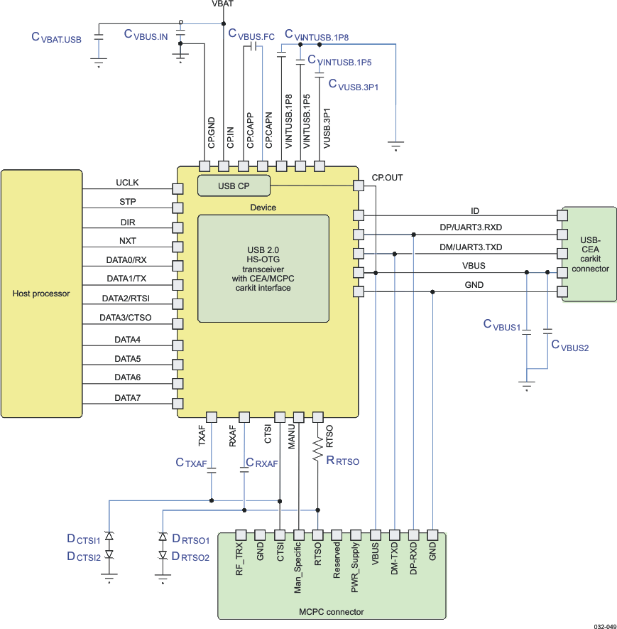 Figure 5-48 USB System Application Schematic
NOTE
For the component values, see Table 5-92.
5.4.2.1 MCPC Carkit Port Timing
MCPC UART specification:
- 11-pin MCPC ARIB-USBI analog carkit interface
- Integrated 50 RRTSO resistor
- UART signaling (from 600 bps to 460.8 kbps)
- Audio (mono/stereo) signaling: In this mode, the ULPI data bus is redefined as a 4-pin UART interface, which exchanges data through a direct access to the FS/LS analog transmitter and receiver.
The UART data are sent and received on the USB D+/D– pads, and the handshake signals are sent and received on the RTSO/CTSI pads.
Figure 5-49 shows the MCPC UART and handshake mode data flow.
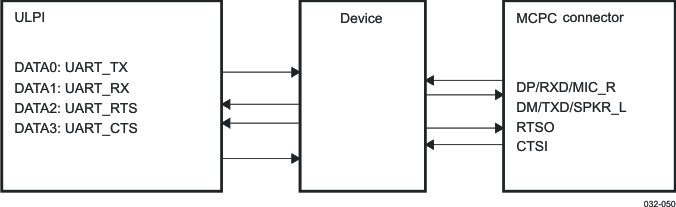 Figure 5-49 MCPC UART and Handshake Mode Data Flow
Table 5-53 lists the McPC UART and handshake mode timings.
Table 5-53 MCPC UART and Handshake Mode Timings
| Notation | Parameter | Min | Max | Unit | |
|---|---|---|---|---|---|
| CK5 | td(UART_TXH-DM) | Delay time, UART_TX rising edge to DM transition | 10 | 37 | ns |
| CK6 | td(UART_TXL-DM) | Delay time, UART_TX falling edge to DM transition | 2.5 | 13 | ns |
| CK7 | td(DPH-UART_RX) | Delay time, DP rising edge to UART_RX transition | 17 | 40 | ns |
| CK8 | td(DPL-UART_RX) | Delay time, DP falling edge to UART_RX transition | 26 | 50 | ns |
| CK9 | td(UART_CTSH-RTSO) | Delay time, UART_CTS rising edge to RTSO transition | 1 | 18 | ns |
| CK10 | td(UART_CTSL-RTSO) | Delay time, UART_CTS falling edge to RTSO transition | 1 | 18 | ns |
| CK11 | td(CTSIH-UART_RTS) | Delay time, CTSI rising edge to UART_RTS transition | 3 | 16 | ns |
| CK12 | td(CTSIL-UART_RTS) | Delay time, CTSI falling edge to UART_RTS transition | 3 | 16 | ns |
Figure 5-50 shows the MCPC UART and handshake mode timings.
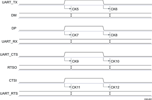 Figure 5-50 MCPC UART and Handshake Mode Timings
5.4.2.2 USB-CEA Carkit Port Timing
CEA carkit mode lets the link communicate through the USB PHY to a remote carkit in CEA audio + data during audio (DDA) mode as defined in the CEA-936A specification. In this mode, the ULPI data bus is redefined as a 2-pin UART interface, which exchanges data through a direct access to the FS/LS analog transmitter and receiver.
UART data are sent and received on the USB D+/D– pads. D+/D– are also used in this mode to carry audio I/O signals.
Table 5-54 assumes testing over the recommended operating conditions (see the CEA-936A specification).
Table 5-54 USB-CEA Carkit Interface Timing Parameters
| Parameter | Min | Max | Unit | |
|---|---|---|---|---|
| tPH_DP_CON | Phone D+ connect time | 100 | ms | |
| tCR_DP_CON | Carkit D+ connect time | 150 | 300 | ms |
| tPH_DM_CON | Phone D– connect time | 10 | ms | |
| tPH_CMD_DLY | Phone command delay | 2 | ms | |
| tPH_MONO_ACK | Phone mono acknowledge | 10 | ms | |
| tPH_DISC_DET | Phone D+ disconnect time | 150 | ms | |
| tCR_DISC_DET | Carkit D– disconnect detect | 50 | 150 | ms |
| tPH_AUD_BIAS | Phone audio bias | 1 | ms | |
| tCR_AUD_DET | Carkit audio detect | 400 | 800 | μs |
| tCR_UART_DET | Carkit UART detect (DDA enabled) | 700 | 1200 | ns |
| tPH_STLO_DET | Phone stereo D+ low detect | 30 | 100 | ms |
| tPH_PLS_POS | Phone D– interrupt pulse width | 200 | 600 | ns |
| tCR_PLS_NEG | Carkit D+ interrupt pulse width | 200 | 600 | ns |
| tDAT_AUD_POL | DDA polarity | 20 | 60 | ms |
| tACC_COL_DET | Accessory identification (ID) collision detect | 2 | 3 | ms |
| tACC_INT_PW | Accessory ID interrupt pulse width | 200 | 400 | μs |
| tACC_INT_WAIT | Accessory ID interrupt wait time | 10 | 15 | ms |
| tACC_CMD_WAIT | Accessory ID command wait time | 0 | ms | |
| tPH_INT_PW | Phone ID interrupt pulse width | 4 | 8 | ms |
| tPH_INT_WAIT | Phone ID interrupt wait time | 4 | 8 | ms |
| tPH_CMD_WAIT | Phone ID command wait time | 0 | ms | |
| tPH_UART_RPT | Phone command repeat time | 50 | ms | |
| tCR_UART_RSP | Carkit UART response | 30 | ms | |
| tCR_INT_RPT | Carkit interrupt repeat time | 50 | ms | |
| fUART_DFLT | Default UART signaling rate (typical rate) | 9600 | bps | |
Figure 5-51 shows the USB-CEA carkit UART data flow.
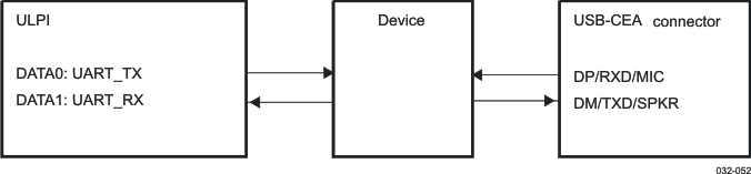 Figure 5-51 USB-CEA Carkit UART Data Flow
Table 5-55 lists the USB-CEA carkit UART timing parameters.
Table 5-55 USB-CEA Carkit UART Timing Parameters
| Notation | Parameter | Min | Max | Unit | ||
|---|---|---|---|---|---|---|
| CK1 | td(UART_TXH-DM) | Delay time, UART_TX rising edge to DM transition | 4.0 | 11 | ns | |
| CK2 | td(UART_TXL-DM) | Delay time, UART_TX falling edge to DM transition | 4.0 | 11 | ns | |
| CK3 | td(DPH-UART_RX) | Delay time, DP rising edge to UART_RX transition | At 38.4 MHz | 205 | 234 | ns |
| At 19.2 MHz | 310 | 364 | ||||
| CK4 | td(DPL-UART_RX) | Delay time, DP falling edge to UART_RX transition | At 38.4 MHz | 205 | 234 | ns |
| At 19.2 MHz | 310 | 364 | ||||
Figure 5-52 shows the USB-CEA carkit UART timings.
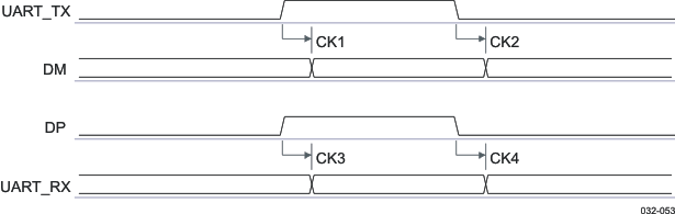 Figure 5-52 USB-CEA Carkit UART Timing Parameters
5.4.2.3 HS USB Port Timing
The ULPI interface supports an 8-bit data bus and the internal clock mode. The 4-bit data bus and the external clock mode are not supported.
The HS functional mode supports an operating rate of 480 Mbps.
Table 5-56 and Table 5-57 assume testing over the recommended operating conditions (see Figure 5-53).
 Figure 5-53 HS USB Interface—Transmit and Receive Modes (ULPI 8-Bit)
NOTE
ULPI data [7:0] lines are set to 1 after USB PHY power up, and before the clock signal is stable.
The input timing requirements are given by considering a rising or falling time of 1 ns.
Table 5-56 HS USB Interface Timing Requirement Parameters
| Notation | Parameter | Min | Max | Unit | |
|---|---|---|---|---|---|
| HSU4 | ts(STPV-CLKH) | Setup time, STP valid before UCLK rising edge | 6 | ns | |
| HSU5 | th(CLKH-STPIV) | Hold time, STP valid after UCLK rising edge | 0 | ns | |
| HSU6 | ts(DATAV-CLKH) | Setup time, DATA[0:7] valid before UCLK rising edge | 6 | ns | |
| HSU7 | th(CLKH-DATIV) | Hold time, DATA[0:7] valid after UCLK rising edge | 0 | ns | |
Table 5-57 HS USB Interface Switching Requirement Parameters(1)
| Notation | Parameter | Min | Typ | Max | Unit | ||
|---|---|---|---|---|---|---|---|
| HSU0 | fp(CLK) | UCLK clock frequency | Steady state | 58.42 | 60 | 61.67 | MHz |
| HSU1 | tW(CLK) | UCLK duty cycle | Steady state | 48.3% | 50% | 51.7% | |
| HSU2 | td(CLKH-DIR) | Delay time, UCLK rising edge to DIR transition | Steady state | 0 | 9 | ns | |
| td(CLKH-NXTV) | Delay time, UCLK rising edge to NXT transition | Steady state | 0 | 9 | ns | ||
| HSU3 | td(CLKH-DATV) | Delay time, UCLK rising edge to DATA[0:7] transition | Steady state | 0 | 9 | ns | |
The capacitive load for the CLK port is 6 pF (rising and falling time is 1 ns).
The HS USB interface has only one state: steady state.
5.4.2.4 PHY Electrical Characteristics
The PHY is the physical signaling layer of the USB 2.0. It contains the drivers and receivers required for physical data and protocol signaling on the DP and DM lines.
The PHY interfaces to the USB controller through UTMI.
There are two main classes of transmitters and receivers in the PHY:
- FS and LS transceivers. These are the legacy USB1.x transceivers.
- HS transceivers
To bias the transistors and run the logic, the PHY also contains reference generation circuitry which consists of:
- A digital phase-locked loop (DPLL) that does a frequency multiplication to achieve the 480-MHz low-jitter lock necessary for USB, and the clock required for the switched capacitor resistance block
- A switched capacitor resistance block that replicates an external resistor on chip
Built-in pullup and pulldown resistors are used as part of the protocol signaling.
The PHY also contains circuitry that protects it from an accidental 5-V short on the DP and DM lines and from 8-kV IEC ESD strikes.
5.4.2.4.1 5-V Tolerance
When the voltage on DP or DM exceeds 3.6 V, a stress condition is detected. In this case, the current is drawn from the DP/DM line, to prevent damage caused by the stress voltage. In this condition, the VRUSB_3V supply can be charged as high as 3.6 V. Table 5-58 lists the tolerances.
Table 5-58 5V-Tolerant Electrical Summary
| Parameter | Comments | Min | Typ | Max | Unit | |
|---|---|---|---|---|---|---|
| Continuous short-circuit stress | DCSTRESS | 50% TX/50% RX/50% LS/50% FS/VBUS = 5.25 V | 24 | h | ||
| Worst case overshoot and undershoot stress | ACSTRESS | tHI = 60 ns/tLO = 100 ns/tR = tF = 4 ns/ VHI = 4.6 V/VLO = –1.0 V/RSRC = 39Ω/ 50% TX/50% RX/VBUS = 5.25 V |
24 | h | ||
| Internal DP/DM stress voltage | VDX_STRESS | Force 5.25 V VBUS/DP/DM | 4.3 | V | ||
| V3P1 stress voltage | V3P1_STRESS | Force 5.25 V VBUS/DP/DM/ID | 3.6 | V | ||
| DP/DM input stress current | IDX_STRESS | Force 5.25 V VBUS/DP/DM | 30 | mA | ||
| ID input stress current | IID_STRESS | Force 5.25 V VBUS/DP/DM/ID | 25 | μA | ||
5.4.2.4.2 LS/FS Single-Ended Receivers
In addition to the differential receiver, there is a single-ended receiver (SE–, SE+) for each of the two data lines D+/–. The main purpose of the single-ended receivers is to qualify the D+ and D– signals in the FS/LS modes of operation. Table 5-59 lists the parameters of the LS/FS single-ended receivers.
Table 5-59 LS/FS Single-Ended Receivers
| Parameter | Comments | Min | Typ | Max | Unit | |
|---|---|---|---|---|---|---|
| USB Single-Ended Receivers | ||||||
| Skew between VP and VM | SKWVP_VM | Driver outputs unloaded | –2 | 0 | 2 | ns |
| Single-ended hysteresis | VSE_HYS | 0 | mV | |||
| High (driven) | VIH | 2 | V | |||
| Low | VIL | 0.8 | V | |||
| Switching threshold | VTH | 0.8 | 2 | V | ||
| UART Receiver CEA | ||||||
| VIH_SER | DP_PULLDOWN asserted | 2 | V | |||
| Serial interface input low | VIL_SER | DP_PULLDOWN asserted | 0.8 | V | ||
| Switching threshold | VTH | 0.8 | 2 | V | ||
| UART Receiver MCPC From DP.RXD | ||||||
| MCPC DP pullup | RMCPCDP | Internal pullup | 4.7k | 10k | Ω | |
| Open-drain input high level | ZIH | Internal MCPC DP pullup asserted | Open | Ω | ||
| Open-drain input low level | ZIL | External open-drain NMOS impedance to ground. With internal MCPC DP pullup asserted. | 100 | Ω | ||
| Output high level | VOH (*) | At DATA1 pin | VIO – 0.45 | V | ||
| Output low level | VOL | At DATA1 pin | 0.45 | V | ||
5.4.2.4.3 LS/FS Differential Receiver
A differential input receiver (RX) retrieves the LS/FS differential data signaling. The differential voltage on the line is converted to digital data by a differential comparator on DP/DM. This data is then sent to a clock and data recovery circuit that recovers the clock from the data. In an additional serial mode, the differential data is directly output on the RXRCV pin. Table 5-60 lists the parameters of the LS/FS differential receiver.
Table 5-60 LS/FS Differential Receiver
| Parameter | Comments | Min | Typ | Max | Unit | |
|---|---|---|---|---|---|---|
| Skew between VP/VM | SKWVP_VM | Driver outputs unloaded | –16 | 0 | 16 | ns |
| Receiver power-up time | TPWR_UP_RCV | 0 | 100 | 200 | μs | |
| Differential common mode range | VCM | 0.8 | 2.5 | V | ||
| Differential input sensitivity | VDI | 0.2 | V | |||
5.4.2.4.4 LS/FS Differential Transmitter
The USB transceiver (TX) uses a differential output driver to drive the USB data signal D+/– onto the USB cable. The driver outputs support 3-state operation to achieve bidirectional half-duplex transactions. Table 5-61 lists the parameters of the LS/FS differential transmitter.
Table 5-61 LS/FS Differential Transmitter
| Parameter | Comments | Min | Typ | Max | Unit | |
|---|---|---|---|---|---|---|
| B-device (dual-role) unconfigured average current | IB_OTG_UNCFG | 0 V = VBUS = 5.25 V, tAVG = 1 ms | 150 | μA | ||
| B-device (secure remote password [SRP] capable, peripheral only) unconfigured average current | IB_PO_UNCFG | 8 | mA | |||
| FS fall time/rise time | tFf, tFr | 10%–90% CL = 50 pF on DP and DM |
4 | 20 | ns | |
| FS rise and fall time matching | TFRFM | 10%–90% CL = 50 pF on DP and DM |
90% | 110% | ||
| FS width of SE0 interval during differential transition | tFst | Pulldowns R = 15 kΩ on DP and DM Pullup R = 1.5 kΩ at 3.6 V on DP only |
14 | ns | ||
| LS fall time/rise time | tLF, tLR | 10%–90% CL = [200–600] pF on DP and DM Pullup R = 1.5 kΩ at 3.6 V for DM only |
75 | 300 | ns | |
| LS rise and fall time matching | TLRFM | 10%–90% CL = [200–600] pF on DP and DM Pullup R = 1.5 kΩ at 3.6 V for DM only |
80% | 120% | ||
| LS width of SE0 interval during differential transition | tLST | Pulldowns R = 15 kΩ on DP and DM Pullup R = 1.5 kΩ at 3.6 V on DM only |
210 | ns | ||
| Driver power-up time | TPWR_UP_TXD | Pulldowns R = 15 kΩ on DP and DM Pullup R = 1.5 kΩ at 3.6 V on DM only |
0 | 100 | 200 | μs |
| FS source driver jitter to next transition | tSDJ1 | CL = 50 pF on DP and DM | –2 | 2 | ns | |
| FS source driver jitter for paired transitions | tSDJ2 | CL = 50 pF on DP and DM | –1 | 1 | ns | |
| LS upstream facing port source driver jitter (next transition) | tUSDJ1 | CL = [200–600] pF on DP and DM Pullup R = 1.5 kΩ at 3.6 V for DM only |
–25 | 25 | ns | |
| LS upstream facing port source driver jitter (next transition) | tUSDJ2 | CL = [200–600] pF on DP and DM Pullup R = 1.5 kΩ at 3.6 V for DM only |
–10 | 10 | ns | |
| Output signal cross-over voltage | Vcrs | Pulldowns R = 15 kΩ on DP and DM Pullup R = 1.5 kΩ at 3.6 V on DM only |
1.3 | 2 | V | |
| High (driven) | VOH | Pulldowns R = 15 kΩ on DP and DM | 2.8 | 3.3 | 3.6 | V |
| Low | VOL | Pullups R = 1.5 kΩ at 3.6 V on DP and DM | 0 | 0.1 | 0.3 | V |
| Driver output resistance | ZDRV/RS | 28 | 36 | 44 | Ω | |
5.4.2.4.5 HS Differential Receiver
The HS receiver consists of the following blocks:
- A differential input comparator to receive the serial data
- A squelch detector to qualify the received data
- An oversampler-based clock data recovery scheme followed by a nonreturn to zero inverted (NRZI) decoder, bit unstuffing, and a serial-to-parallel converter to generate the UTMI DATAOUT
Table 5-62 lists the parameters of the HS differential receiver.
Table 5-62 HS Differential Receiver
| Parameter | Comments | Min | Typ | Max | Unit | |
|---|---|---|---|---|---|---|
| Input Levels for HS | ||||||
| HS squelch detection threshold | VHSSQ | (Differential signal amplitude) | 100 | 125 | 150 | mV |
| HS disconnect detection threshold | VHSDSC | (Differential signal amplitude) | 525 | 600 | 625 | mV |
| HS data signaling common mode voltage range | VHSCM | –50 | 200 | 500 | mV | |
| HS differential input sensitivity | VDIHS | (Differential signal amplitude) | –100 | 100 | mV | |
| Input Impedance for HS | ||||||
| Internal specification for input capacitance | CHSLOAD | 11 | pF | |||
| Internal CHSLOAD DP/DM matching | CHSLOADM | 0.2 | pF | |||
| External Components With the Total Budget Combined (Without USB Cable Load) | ||||||
| External capacitance on DP or DM | 2 | pF | ||||
| External series resistance on DP or DM | 1 | Ω | ||||
5.4.2.4.6 HS Differential Transmitter
The HS transmitter is always operated on the UTMI parallel interface. The parallel data on the interface is serialized, bit-stuffed, NRZI-encoded, and transmitted as a dc output current on DP or DM, depending on the data. Each line has an effective 22.5-Ω load to ground, which generates the voltage levels for signaling.
A disconnect detector is also part of the HS transmitter. A disconnect on the far end of the cable causes the impedance seen by the transmitter to double, thereby doubling the differential amplitude seen on the DP/DM lines.
Table 5-63 lists the parameters of the HS differential transmitter.
Table 5-63 HS Differential Transmitter
| Parameter | Comments | Min | Typ | Max | Unit | |
|---|---|---|---|---|---|---|
| Output Levels for HS | ||||||
| HS TX idle level | VHSOI | Absolute voltage DP/DM – Both internal/external 45 Ω | –10 | 0 | 10 | mV |
| HS TX data signaling high | VHSOH | Absolute voltage DP/DM – Both internal/external 45 Ω | 360 | 400 | 440 | mV |
| HS data signaling low | VHSOL | –10 | 0 | 10 | mV | |
| Chirp J level | VCHIRPJ | Differential voltage | 700 | 800 | 1100 | mV |
| Chirp K level | VCHIRPK | Differential voltage | –900 | –800 | –500 | mV |
| HS TX disconnect threshold | VDISCOUT | Absolute voltage DP/DM—No external 45 Ω | 700 | mV | ||
| Driver Characteristics | ||||||
| Rise time | tHSR | (10%–90%) | 500 | ps | ||
| Fall time | tHSF | (10%–90%) | 500 | ps | ||
| Driver output resistance | ZHSDRV | Also serves as HS termination | 40.5 | 45 | 49.5 | Ω |
5.4.2.4.7 CEA/MCPC/UART Driver
Table 5-64 lists the parameters of the CEA/MCPC/UART driver.
Table 5-64 CEA/MCPC/UART Driver
| Parameter | Comments | Min | Typ | Max | Unit | |
|---|---|---|---|---|---|---|
| UART Driver CEA | ||||||
| Phone UART edge rates | tPH_UART_EDGE | DP_PULLDOWN asserted | 1 | μs | ||
| Serial interface output high | VOH_SER | ISOURCE = 4 mA | 2.4 | 3.3 | 3.6 | V |
| Serial interface output low | VOL_SER | ISINK = –4 mA | 0 | 0.1 | 0.4 | V |
| UART Driver MCPC to DM.TX. | ||||||
| Input high level | VIH (*) | At DATA0 pin | VIO – 0.45 | V | ||
| Input low level | VIL | At DATA0 pin | 0.45 | V | ||
| MCPC DM external pullup | RMCPCDM | External pullup | 4.7k | 10k | Ω | |
| MCPC DM pullup supply | MCPCVDDEXT | External pullup supply | 1.8 | 3.3 | V | |
| Open-drain output high level | ZOH | External pullup asserted | HiZ | Ω | ||
| HiZ means high impedance equivalent to open | ||||||
| Open-drain output low level | VOL | With open-drain NMOS to ground is ON and external pullup is asserted. | 0 | 0.6 | V | |
| Carkit Pulse Driver | ||||||
| Pulse match tolerance | QPLS_MTCH | ZCR_SPKR_IN = 60 kΩ at f = 1 kHz | 5% | |||
| Phone D– interrupt pulse width | tPH_PLS_POS | ZCR_SPKR_IN = 60 kΩ at f = 1 kHz | 200 | 600 | ns | |
| Phone positive pulse voltage | VPH_PLS_POS | ZCR_SPKR_IN = 60 kΩ at f = 1 kHz | 2.8 | 3.6 | V | |
5.4.2.4.8 Pullup/Pulldown Resistors
Table 5-65 lists the parameters of the pullup/pulldown resistors.
Table 5-65 Pullup/Pulldown Resistors
| Parameter | Comments | Min | Typ | Max | Unit | |
|---|---|---|---|---|---|---|
| Pullup Resistors | ||||||
| Bus pullup resistor on upstream port (idle bus) | RPUI | Bus idle | 0.9 | 1.1 | 1.575 | kΩ |
| Bus pullup resistor on upstream port (receiving) | RPUA | Bus driven/driver outputs unloaded | 1.425 | 2.2 | 3.09 | |
| High (floating) | VIHZ | Pullups/pulldowns on DP and DM lines | 2.7 | 3.6 | V | |
| Phone D+ pullup voltage | VPH_DP_UP | Driver outputs unloaded | 3 | 3.3 | 3.6 | V |
| Pulldown Resistors | ||||||
| Phone D+/– pulldown | RPH_DP_DWN | Driver outputs unloaded | 14.25 | 18 | 24.8 | kΩ |
| RPH_DM_DWN | ||||||
| High (floating) | VIHZ | Pullups/pulldowns on DP and DM lines | 2.7 | 3.6 | V | |
| D+/– Data Line | ||||||
| Upstream facing port | CINUB | 22 | 75 | pF | ||
| OTG device leakage | VOTG_DATA_LKG | 0.342 | V | |||
| Input impedance exclusive of pullup/pulldown(1) | ZINP | Driver outputs unloaded (waiver from usb.org standards committee) | 80 | 120 | kΩ | |
5.4.2.4.9 PHY DPLL Electrical Characteristics
USB DPLL supports input frequencies of 12, 13, 19.2, 24, and 26 MHz. The input frequency must be programmed through frequency select bits. USB DPLL provides a low jitter and gives eight equidistant phases of the 480-MHz clock for the USB receiver.
Table 5-66 lists the electrical characteristics of the PHY DPLL.
Table 5-66 PHY DPLL Electrical Characteristics
| Parameter | Comments | Min | Typ | Max | Unit | |
|---|---|---|---|---|---|---|
| Input clock | 12 | MHz | ||||
| 13 | ||||||
| 19.2 | ||||||
| 24 | ||||||
| 26 | ||||||
| Digital supply | VINTDIG | 1.35 | 1.5 | 1.65 | V | |
| Analog 1.5-V supply | VRUSB_1V5 | 1.35 | 1.5 | 1.65 | V | |
| Analog 1.8-V supply | VRUSB_1V8 | 1.62 | 1.8 | 1.98 | V | |
| Output frequency (eight phases) | 480 | MHz | ||||
| RMS period jitter (output) | 10 | ps | ||||
| Deterministic period jitter (output) | 50 | ps | ||||
| RMS jitter per phase noise frequency band (input) | Frequency band: 1 to 10 Hz | 310 | ps | |||
| Frequency band: 10 to 100 Hz | 90 | |||||
| Frequency band: 100 to 1000 Hz | 30 | |||||
| Frequency band: 1 to 10 kHz | 10 | |||||
| Frequency band: 10 to 100 kHz | 10 | |||||
| Frequency band: 0.1 to 0.5 MHz | 290 | |||||
| Frequency band: 0.5 to 1 MHz | 650 | |||||
| Deterministic period jitter (input) | 100 | ps | ||||
| Frequency error (input) | ±150 | ppm | ||||
| Frequency error (output) | ±500 | ppm | ||||
| Phase-to-phase variation | 35 | ps | ||||
| Noise on digital 1.5-V supply | 100 | mV | ||||
| Noise on analog 1.5-V supply | 50 | mV | ||||
| Noise on analog 1.8-V supply | 36 | mV | ||||
5.4.2.4.10 PHY Power Consumption
Table 5-67 lists, by mode, the power consumption values of the modules.
Table 5-67 PHY Power Consumption
| Supply | Min | Typ | Max | Unit |
|---|---|---|---|---|
| HS Mode | ||||
| VUSB.3P1 | 8.5 | mA | ||
| VINTUSB1P8.OUT | 25 | mA | ||
| VINTUSB1P5.OUT | 24 | mA | ||
| VINTDIG.OUT | 0.3 | mA | ||
| FS Mode | ||||
| VUSB.3P1 | 13 | mA | ||
| VINTUSB1P8.OUT | 5.4 | mA | ||
| VINTUSB1P5.OUT | 17.5 | mA | ||
| VINTDIG.OUT | 0.3 | mA | ||
| LS Mode | ||||
| VUSB.3P1 | 12.5 | mA | ||
| VINTUSB1P8.OUT | 5.4 | mA | ||
| VINTUSB1P5.OUT | 17.5 | mA | ||
| VINTDIG.OUT | 0.3 | mA | ||
| Low-Power/Suspend Mode | ||||
| VUSB.3P1 | 0 | mA | ||
| VINTUSB1P8.OUT | 0 | mA | ||
| VINTUSB1P5.OUT | 2 | μA | ||
| VINTDIG.OUT | 0 | mA | ||
| Power-Down Mode | ||||
| VUSB.3P1 | 0 | mA | ||
| VINTUSB1P8.OUT | 0 | mA | ||
| VINTUSB1P5.OUT | 2 | μA | ||
| VINTDIG.OUT | 0 | mA |
5.4.2.5 OTG Electrical Characteristics
The OTG block integrates three main functions:
- USB plug detection function on VBUS and ID
- ID resistor detection
- VBUS level detection
5.4.2.5.1 OTG VBUS Electrical
Table 5-68 lists the OTG VBUS electrical parameters.
Table 5-68 OTG VBUS Electrical
| Parameter | Comments | Min | Typ | Max | Unit | |
|---|---|---|---|---|---|---|
| VBUS Wake-Up Comparator | ||||||
| VBUS wake-up delay | DELVBUS_WK_UP | 15 | μs | |||
| VBUS wake-up threshold | VVBUS_WK_UP | 0.5 | 0.6 | 0.7 | V | |
| VBUS Comparators | ||||||
| A-device session valid | VA_SESS_VLD | 0.8 | 1.1 | 1.4 | V | |
| A-device VBUS valid | VA_VBUS_VLD | 4.4 | 4.5 | 4.6 | V | |
| B-device session end | VB_SESS_END | 0.2 | 0.5 | 0.8 | V | |
| B-device session valid | VB_SESS_VLD | 2.1 | 2.4 | 2.7 | V | |
| VBUS Line | ||||||
| A-device VBUS input impedance to ground | RA_BUS_IN | SRP (VBUS pulsing) capable A-device not driving VBUS | 100 | kΩ | ||
| B-device VBUS SRP pulldown | RB_SRP_DWN | 5.25 V/8 mA, pullup voltage = 3 V | 0.656 | 10 | kΩ | |
| B-device VBUS SRP pullup | RB_SRP_UP | (5.25 V – 3 V)/8 mA, pullup voltage = 3 V | 0.281 | 1 | 2 | kΩ |
| B-device VBUS SRP rise time maximum for OTG-A communication | tRise_SRP_UP_Max | 0 to 2.1 V with < 13 μF load | 36 | ms | ||
| B-device VBUS SRP rise time minimum for standard host connection | tRise_SRP_UP_Min | 0.8 to 2.0 V with > 97 μF load | 60 | ms | ||
| VBUS line maximum voltage | If VBUS_CHRG bit is low* | 7 | V | |||
5.4.2.5.2 OTG ID Electrical
Table 5-69 lists the OTG ID electrical parameters.
Table 5-69 OTG ID Electrical
| Parameter | Comments | Min | Typ | Max | Unit | |
|---|---|---|---|---|---|---|
| ID Wake-Up Comparator | ||||||
| ID wake-up comparator | RID_WK_UP | Wake up when ID shorted to ground through a resistor lower than 445 kΩ (±1%) | 445 | kΩ | ||
| ID Comparators—ID External Resistor Specifications | ||||||
| ID ground comparator | RID_GND | ID_GND interrupt when ID shorted to ground through a resistor lower than 10 Ω | 0 | 5 | 10 | Ω |
| ID 100k comparators | RID_100K | ID_100K interrupt when 102 kΩ (1%) resistor plugged in | 101 | 102 | 103 | kΩ |
| ID 200k comparators | RID_200K | ID_200K interrupt when 200 kΩ (1%) resistor plugged in | 198 | 200 | 202 | kΩ |
| ID 440k comparators | RID_440K | ID_440K interrupt when 440 kΩ (1%) resistor plugged in | 435 | 440 | 445 | kΩ |
| ID float comparator | RID_FLOAT | ID_FLOAT interrupt when ID shorted to ground through a resistor higher than 560 kΩ | 1400 | kΩ | ||
| ID Line | ||||||
| Phone ID pullup to VPH_ID_UP | RPH_ID_UP | ID unloaded (VRUSB) | 70 | 200 | 286 | kΩ |
| Phone ID pullup voltage | VPH_ID_UP | Connected to VRUSB | 2.5 | 3.2 | V | |
| ID line maximum voltage | 5.25 | V | ||||
5.5 Battery Interface
5.5.1 General Description
5.5.1.1 Battery Charger Interface Overview
The TPS65950 has a BCI for complete battery management. The main function of the BCI is to control the charging of either 1-cell Li-ion or Li-ion polymer batteries, or 1-cell Li-ion batteries with cobalt-nickel-manganese anodes. It supports regulated ac chargers of 7-V absolute maximum and can charge with USB host devices, MCPC devices, USB chargers, or carkits of 7-V absolute maximum. The BCI can perform software-controlled linear charging with the sources mentioned, software-controlled pulsed charging with current-limited ac chargers, and automatic linear charging with ac chargers, USB chargers, and carkits.
The battery is monitored using the 10-bit ADC from the MADC to measure battery voltage, battery temperature, battery type, battery charge current, USB device input voltage, and ac charger input voltage. The magnitude of the charging current and the charging voltage is set by 10 bits of a programming register converted by a 10-bit DAC, whose output sets the reference input of the charging current and charging voltage control loop.
The BCI also performs monitoring functions:
- ac charger detection
- VBUS detection
- Battery detection
- ac charger overvoltage detection
- VBUS overvoltage detection
- Battery overvoltage detection
- Battery voltage level detection
- Battery charge current level detection
- Battery temperature out-of-range detection
- Battery end-of-charge detection
- Battery overcurrent detection
- Watchdog
5.5.1.2 Battery Backup Overview
The TPS65950 implements a backup mode, in which the backup battery keeps the RTC running. A rechargeable backup battery can be recharged from the main battery.
When the main battery is below 2.7 V or is removed, the backup battery powers the backup if the backup battery voltage is greater than 1.8 V. The backup domain powers up the following:
- Internal 32.768-kHz oscillator
- RTC
- Hash table (20 registers of 8 bits each)
- Eight GP storage registers
5.5.2 Typical Application Schematics
5.5.2.1 Functional Configurations
The BCI can be used in different configurations (see Figure 5-54). Each configuration requires a dedicated typical application schematic:
- ac charge supported (see Figure 5-54A, Figure 5-54B, and Figure 5-54D)
- USB charge supported (see Figure 5-54A and Figure 5-54C)
- ac constant voltage mode supported (see Figure 5-54A and Figure 5-54B)
- ac charger with current nonlimited (see Figure 5-54D)
NOTE
For the component values, see Table 5-92.
5.5.2.2 In-Rush Current Limitation Schematic
With the typical application schematic supporting constant voltage mode (Figure 5-54 A and B), battery in-rush current is limited by the charging device. The application schematic can be enhanced to support in-rush current at the charging device plug to maximum 850 mA as detailed by Figure 5-55. T3, R3, and C3 are connected between VAC and ICTLAC1 and intentionally bring in-rush cucation. The described enhancement is not required for Figure 5-54 D, where constant voltage mode is not supported.
Figure 5-55 shows a typical application schematic with in-rush current limitation.
 Figure 5-55 Typical Application Schematic (In-Rush Current Limitation)
5.5.2.3 Configuration With BCI Not Used
Figure 5-56 shows how to connect the BCI when it is not in use. The SUSPENDM bit must be set to disable the BCI internally.
 Figure 5-56 Typical Application Schematic (BCI Not Used)
5.5.3 Electrical Characteristics
This section describes the electrical characteristics of the BCI in the TPS65950.
5.5.3.1 Main Charge
Table 5-70 lists the electrical characteristics of the main charge.
Table 5-70 Main Charge Electrical Characteristics
VBAT = 3.6 V, RS = 0.22 Ω, unless otherwise specified
| Parameter | Test Conditions | Min | Typ | Max | Unit |
|---|---|---|---|---|---|
| VAC input voltage range(1) | dc voltage | 4.8 | 5.4 | 7 | V |
| VBUS input voltage range (external) | dc voltage | 4.4 | 5 | 7 | V |
| Charge current range | 1.7 | A | |||
| VAC accessory supply mode consumption | VBAT = 3.6 V, consumption on VBAT when ACCSUPEN = 1 and ACPATHEN = 1 connected to VBAT, current limitation enabled | 0.75 | 1 | mA | |
| VBAT = 3.6 V, consumption on VBAT when ACCSUPEN = 1 and ACPATHEN = 1 connected to VBAT, current limitation disabled | 0.525 | 0.7 | |||
| VBUS accessory supply mode consumption | VBAT = 3.6 V, consumption on VBAT when ACCSUPEN = 1 and USBPATHEN = 1 connected to VBAT, current limitation enabled | 0.64 | 0.85 | mA | |
| VBAT = 3.6 V, consumption on VBAT when ACCSUPEN = 1 and USBPATHEN = 1 connected to VBAT, current limitation disabled | 0.415 | 0.55 | |||
| ICTLAC1 output voltage swing (PWM charge) | IICTLAC1 = –10 μA, ACPATHEN = 1, PWMEN = 1, PWMDTYCY = 0x000 |
VAC–0.3 | V | ||
| IICTLAC1 = 10 μA, ACPATHEN = 1, PWMEN = 1, PWMDTYCY = 0x3FF |
0.35 | ||||
| ICTLAC1 output voltage swing (linear charge) | IICTLAC1 = –10 μA, ACPATHEN = 1, LINCHEN = 1, MESBAT = 1, CHGVREG = 0x000 |
VAC–0.3 | V | ||
| IICTLAC1 = 10 μA, ACPATHEN = 1, LINCHEN = 1, MESBAT = 1, CHGVREG = 0x3FF |
0.35 | ||||
| ICTLUSB1 output voltage swing (linear charge) | IICTLUSB1 = –10 μA, USBPATHEN = 1, LINCHEN = 1, MESBAT = 1, CHGVREG = 0x000 |
VBUS–0.3 | V | ||
| IICTLUSB1 = 10 μA, USBPATHEN = 1, LINCHEN = 1, MESBAT = 1, CHGVREG = 0x3FF |
0.35 | ||||
| ICTLAC2 output voltage swing (linear charge) | IICTLAC2 = –10 μA, ACPATHEN = 1, LINCHEN = 1, ACPATHEN = 0 |
VCCS–0.3 | V | ||
| IICTLAC2 = 10 μA, ACPATHEN = 1, LINCHEN = 1, ACPATHEN = 1 |
0.35 | ||||
| ICTLUSB2 output voltage swing (linear charge) | IICTLUSB2 = –10 μA, USBPATHEN = 1, LINCHEN = 1, USBPATHEN = 0 |
VCCS–0.3 | V | ||
| IICTLUSB2 = 10 μA, USBPATHEN = 1, LINCHEN = 1, USBPATHEN = 1 |
0.35 | ||||
| PWM mode output current | PWM = 1 (ICTLAC1 = 0), VAC = 6.8 V | 5.0 | mA | ||
| PWM = 0 (ICTLAC1 = VAC), VAC = 6.8 V | –2.0 | ||||
| ac main charge battery removal switch-off time | CHGIREG = (value relative to ICHG = 0.6 A), VAC = 5.4 V, C = 100 nF connected to ICTLAC1, VBAT threshold = 4.55 V, measure charge current from removal to 10% Miller compensation |
150 | μs | ||
| CHGIREG = (value relative to ICHG = 0.6 A), VAC = 5.4 V, C = 100 nF connected to ICTLAC1, VBAT threshold = 4.55 V, measure charge current from removal to 10% Regular compensation |
150 | ||||
| USB main charge battery removal switch-off time | CHGIREG = (value relative to ICHG = 0.6 A), VBUS = 5.0 V, C = 100 nF connected to ICTLUSB1, VBAT threshold = 4.55 V, measure charge current from removal to 10% |
150 | μs | ||
| VAC-to-MADC input attenuation | VAC from 4.8 V to 6.8 V (maximum MADC input voltage = 1.224 V) | 0.12 | 0.15 | 0.18 | V/V |
| VBAT-to-MADC input attenuation | VBAT from 3.0 V to 4.5 V (maximum MADC input voltage = 1.35 V) | 0.2 | 0.25 | 0.3 | V/V |
| Current-to-voltage conversion slope(2) | (VCCS–VBATS) rising from 0 V to 0.17 V: CGAIN = 0 equivalent to 0–775 mA range | 0.704 | 0.88 | 1.056 | mV/mA |
| (VCCS–VBATS) rising from 0 V to 0.33 V: CGAIN = 1 equivalent to 0–1500 mA range | 0.352 | 0.44 | 0.528 | ||
| Current-to-voltage conversion positive offset | OFFSEN = 1, OFFSN[1:0] = 00, CGAIN = 0, OFFSIGN = 0 | 18.7 | mV | ||
| OFFSEN = 1, OFFSN[1:0] = 01, CGAIN = 0, OFFSIGN = 0 | 38.8 | ||||
| OFFSEN = 1, OFFSN[1:0] = 10, CGAIN = 0, OFFSIGN = 0 | 60.1 | ||||
| OFFSEN = 1, OFFSN[1:0] = 11, CGAIN = 0, OFFSIGN = 0 | 82.6 | ||||
| Current-to-voltage conversion negative offset | OFFSEN = 1, OFFSN[1:0] = 00, CGAIN = 0, OFFSIGN = 1 | –18.2 | mV | ||
| OFFSEN = 1, OFFSN[1:0] = 01, CGAIN = 0, OFFSIGN = 1 | –35.6 | ||||
| OFFSEN = 1, OFFSN[1:0] = 10, CGAIN = 0, OFFSIGN = 1 | –52.2 | ||||
| OFFSEN = 1, OFFSN[1:0] = 11, CGAIN = 0, OFFSIGN = 1 | –67.6 | ||||
| Charge voltage and charge current DAC | Linear range | 1FF | 3BA | hex | |
| Differential nonlinearity | –2 | 2 | LSB | ||
| Integrated nonlinearity | –2 | 2 | LSB | ||
| Offset | –25 | 25 | mV | ||
| ADIN0 dc current source | ADIN0 = 1 V | 7 | 10 | 13 | μA |
| ADCIN1 dc current source | ADCIN1 = 1 V, ITHSENS[2:0] = 000 (maximum MADC input voltage = 0.875 V), After TRIM done by ISRCTRIM[3:0], at ambient temperature |
9.875 | 10 | 10.125 | μA |
| ADCIN1 dc current source for temperature measurement | ADCIN1 = 1 V, ITHSENS[2:0] = 000 (maximum MADC input voltage = 0.875 V), after TRIM done by ISRCTRIM[3:0] | 9.5 | 10 | 10.5 | μA |
| ITHSENS[2:0] = 001 | 14 | 20 | 26 | ||
| ITHSENS[2:0] = 010 | 21 | 30 | 39 | ||
| ITHSENS[2:0] = 011 | 28 | 40 | 52 | ||
| ITHSENS[2:0] = 100 | 35 | 50 | 65 | ||
| ITHSENS[2:0] = 101 | 42 | 60 | 78 | ||
| ITHSENS[2:0] = 110 | 49 | 70 | 91 | ||
| ITHSENS[2:0] = 111 | 56 | 80 | 104 | ||
| Constant current loop accuracy | After trimming (±1.10%), VAC = 5.4 V or VBUS = 5.0 V, VBAT = 3.6 V, CHGIREG = (value relative to ICHG = 0.6 A), VCCS–VBATS rising voltage, monitoring ICTLAC1 or ICTLUSB1, CGAIN = 1, overtemperature (ambient 0°C to 50°C) (including the bandgap accuracy overtemperature ±0.5% and the Rsense resistor accuracy ±1%) | –11% | 11% | ||
| After trimming (±0.55%), VAC = 5.4 V or VBUS = 5.0 V, VBAT = 3.6 V, CHGIREG = (value relative to ICHG = 0.6 A), VCCS–VBATS rising voltage, monitoring ICTLAC1 or ICTLUSB1, CGAIN = 0, overtemperature (ambient 0°C to 50°C) (including the bandgap accuracy overtemperature ±0.5% and the Rsense resistor accuracy ±1%) | –3.15% | 3.15% | |||
| Constant current loop offset | At error amplifier input, before loop trim. Including DAC offset, I-to-V offset after I-to-V trim, error amplifier offset | –46.8 | 46.8 | mV | |
| Constant voltage loop accuracy | After trimming (±0.14%), VAC = 5.4 V or VBUS = 5.0 V, at room temperature, CHGVREG = (value relative to VBAT = 4.37 V), VBAT rising voltage, monitoring ICTLAC1 or ICTLUSB1 | –0.28% | 0.28% | ||
| After trimming (±0.14%), VAC = 5.4 V or VBUS = 5.0 V overtemperature (ambient 0°C to 50°C), CHGVREG = (value relative to VBAT = 4.37 V), VBAT rising voltage, monitoring ICTLAC1 or ICTLUSB1 (including the bandgap accuracy overtemperature ±0.5%) | –0.82% | 0.82% | |||
| Charger presence detect threshold | VBAT = 3.6 V, rising edge | VBAT+0.3 | VBAT+0.4 | VBAT+0.6 | V |
| VBAT = 3.6 V, falling edge | VBAT | VBAT+0.1 | VBAT+0.3 | ||
| Battery threshold when default value(3) | VAC = 5.4 V or VBUS = 5.0 V, VBATOVEN = 1, VBATOVTH(3:0) = default, MESBAT = 1, VBAT rising voltage, monitoring VBATOV status signal | 4.45 | 4.55 | 4.65 | V |
| ac charger overvoltage threshold when default value(3) | VBAT = 3.6 V, VACCHGOVEN = 1, VACCHGOVTH(3:0) = default, VAC rising voltage, monitoring VACCHGOV status signal | 6.24 | 6.5 | 7 | V |
| VBUS overvoltage threshold when default value(3) | VBAT = 3.6 V, VBUSOVEN = 1, VBUSOVTH(3:0) = default, VBUS rising voltage, monitoring VBUSOV status signal | 5.28 | 5.5 | 5.9 | V |
| Main charge main battery presence impedance detection threshold | Measured through ADCIN1 rising voltage and sourced current, monitoring BATSTS value | 67.5 | 75 | 82.5 | kΩ |
| Main charge main battery presence voltage detection threshold | Force ADCIN1 voltage, monitor BATSTS value | 750 | mV | ||
| Temperature detection accuracy | For low temperature (2°C/3°C) For high temperature (43°C/50°C) |
–3 –5 |
3 5 |
°C | |
| Battery voltage accuracy | Tested for VBAT = 2.9, 3.6, and 4.2 V | VBAT–0.1 | VBAT | VBAT+0.1 | V |
| Current charge accuracy | Tested for ICHG = 600 mA | ICHG–0.04 | ICHG | ICHG+0.04 | A |
| Battery Rs | ESR (including FUSE) | 0.5 | Ω |
VBATMAX + 2 PMOS drop + 0.22 Ω resistor drop
(where VBATMAX is the maximum voltage value of the battery; that is, 4.2 V for Li-ion battery)
User must consider maximum dissipation while using maximum ac/USB voltage (7 V) or maximum current load (1.7 A).
MADC output code = (VCCS – VBATS) × 2 with CGAIN = 1
5.5.3.2 Precharge
During slow precharge and fast precharge, a precharge voltage loop is always enabled and limits the battery voltage charge to 3.6 V typical. To use the constant voltage loop, a battery voltage prescaler is also always enabled. The voltage loop is nonlinear. A fast comparator switches off the external power portable media operating system (PMOS) when VBAT is higher than 3.6 V and switches on the PMOS when VBAT is lower than 3.6 V. When the USB charger is used, fast precharge is not available (to comply with USB standards).
In precharge mode, the threshold of the ac charger overvoltage detection is forced to 6.8 V.
Table 5-71 lists the precharge electrical characteristics.
Table 5-71 Precharge Electrical Characteristics
RS = 0.22 Ω, unless otherwise specified
| Parameter | Test Conditions | Min | Typ | Max | Unit |
|---|---|---|---|---|---|
| ICTLAC1 output voltage swing (precharge) | IICTLAC1 = –10 μA, VBAT = 1.5 V, VCCS = VBAT+200 mV, VAC = 5.4 V, SYSACTIV = 0 |
VAC–0.3 | V | ||
| IICTLAC1 = 10 μA, VBAT = 1.5 V, VCCS = VBAT, VAC = 5.4 V, SYSACTIV = 0 |
0.35 | ||||
| ICTLUSB1 output voltage swing (precharge) | IICTLUSB1 = –10 μA, VBAT = 1.5 V, VCCS = VBAT+200 mV, VAC = 0.0 V, VBUS = 5 V, SYSACTIV = 0 |
VAC–0.3 | V | ||
| IICTLUSB1 = 10 μA, VBAT = 1.5 V, VCCS = VBAT, VAC = 0.0 V, VBUS = 5 V, SYSACTIV = 0 |
0.35 | ||||
| ICTLAC2 output voltage swing (precharge) | IICTLAC2 = –10 μA, VBAT = 1.5 V, VCCS = VBAT+200 mV, VAC = 5.4 V, SYSACTIV = 0 |
VCCS–0.3 | V | ||
| IICTLAC2 = 10 μA, VBAT = 1.5 V, VCCS = VBAT, VAC = 5.4 V, SYSACTIV = 0 |
0.35 | ||||
| ICTLUSB2 output voltage swing (precharge) | IICTLUSB2 = –10 μA, VBAT = 1.5 V, VCCS = VBAT+200 mV, VAC = 0.0 V, VBUS = 5 V, SYSACTIV = 0 |
VCCS–0.3 | V | ||
| IICTLUSB2 = 10 μA, VBAT = 1.5 V, VCCS = VBAT, VAC = 0.0 V, VBUS = 5 V, SYSACTIV = 0 |
0.35 | ||||
| ac precharge battery removal switch-off time | In fast precharge, Rlimit = 700 kΩ, VAC = 5.4 V, VBAT threshold = 3.6 V, measure charge current from removal to 10% |
150 | μs | ||
| USB precharge battery removal switch-off time | In precharge, Rlimit = 500 kΩ, VBUS = 5.0 V, VBAT threshold = 3.6 V, measure charge current from removal to 10% |
150 | μs | ||
| PCHGPOR voltage threshold | VAC = 5.4 V or VBUS = 5.0 V, PCHGPOR raise when VPRECH voltage higher than the voltage threshold | 1.2 | V | ||
| PCHGCLK click frequency | VAC = 5.4 V or VBUS = 5.0 V (including temperature variation) | 18.5 | 32 | 45.4 | kHz |
| VAC = 5.4 V or VBUS = 5.0 V (at room temperature) | 24.3 | 32 | 39.68 | ||
| PCHGVREF band gap voltage | VAC = 5.4 V or VBUS = 5.0 V | 0.7125 | 0.75 | 0.7875 | V |
| VPRECH regulator output | VAC = 5.4 V or VBUS = 5.0 V | 1.4 | 1.5 | 1.6 | V |
| Small precharge output current | VBAT = 0.0 V, VAC = 5.4 V or (VBUS = 5.0 V and USBSLOWPCHG = 1) | 3 | 5 | 7 | mA |
| Slow precharge loop accuracy | After TRIMinG, VAC = 5.4 V or VBUS = 5.0 V, VBAT = 1.5 V, VCCS–VBATS rising voltage, monitoring ICTLAC1 or ICTLUSB1 |
14 | 17.2 | 20.3 | mV |
| Fast precharge loop accuracy | After TRIMinG, PCHGAC or PCHGUSB floating, VAC = 5.4 V, VBAT = 3.0 V, VCCS–VBATS rising voltage, monitoring ICTLAC1 or ICTLUSB1 |
56 | 68.8 | 81.2 | mV |
| Precharge constant voltage loop limitation | System did not start after VBAT > 3.2 V, VBATS input. | 3.4 | 3.6 | 3.8 | V |
| VBUSOVPRECH threshold (for USB reliability) | VBUS input | 5.04 | 5.25 | 5.46 | V |
| ac charger overvoltage threshold | VBAT = 2.8 V, VAC input | 6.5 | 6.8 | 7.3 | V |
| VBUS overvoltage threshold | VBAT = 2.8 V, VBUS input | 6.5 | 6.8 | 7.3 | V |
| Battery voltage threshold to start ac fast precharge | VBATS input | 1.8 | 2.0 | 2.2 | V |
| Battery voltage threshold to start ac slow precharge | VBATS input | 1.0 | 1.2 | 1.4 | V |
| Charger presence detect threshold | VBATS = 2.8 V, rising edge | VBAT+0.3 | VBAT+0.4 | VBAT+0.6 | V |
| VBATS = 2.8 V, falling edge | VBAT | VBAT+0.1 | VBAT+0.3 | ||
| VBUS presence detect threshold | Rising edge | 4.4 | V | ||
| Falling edge | 4.3 | ||||
| BCIAUTO detection impedance threshold | To obtain CVENACA = BCIAUTOACA = 0 | 10 | kΩ | ||
| To obtain CVENACA = BCIAUTOACA = 1 | 140 | ||||
| BCIAUTO detection voltage threshold | CVENACA = 0 below the voltage threshold | 100 | 150 | 200 | mV |
| CVENACA = 1 below the voltage threshold | 700 | 750 | 800 | ||
| BCIAUTO detection output current | Measured on BCIAUTO pin | 4.5 | 7.5 | 9.5 | μA |
| Precharge main battery presence impedance detection threshold | Measured through ADCIN1 rising voltage and sourced current, monitoring BATSTS value | 115 | 140 | 192 | kΩ |
| Precharge main battery presence voltage detection threshold | Force ADCIN1 voltage, monitor BATSTS value. | 750 | mV | ||
| Precharge main battery presence detection output current | Measured on ADCIN1 pin | 5.5 | μA |
5.5.3.3 Constant Voltage Mode
The BCI supports a constant voltage (CV) mode. CV mode is automatically started when there is no battery pack, a regulated ac charger is plugged in, and CVENAC = 1. The charging device outputs a constant voltage at the VBAT node. To start CV mode, the precharge analog hardware detects whether a battery pack is open using the battery presence comparator, and detects whether an ac charger is connected using the ac charger presence comparator.
CV mode is disabled when VAC is greater than 6.5 V typical. ac overvoltage protection is also enabled during CV mode.
Hardware implementation for CV mode uses the main charge constant voltage loop. In CV mode, a 35-mA typical load is synced internally to keep the regulated VBAT voltage output stable. An 80-μF typical external capacitor must be connected to the VBAT node.
Table 5-72 lists the electrical characteristics of CV mode.
Table 5-72 CV Mode Electrical Characteristics(1)
| Parameter | Test Conditions | Min | Typ | Max | Unit |
|---|---|---|---|---|---|
| Main charge constant voltage mode | VAC = 5.4 V, ADCIN1 pin floating, LDOOK = 1 | ||||
| CBAT | Battery node capacitor | 37 | 80 | 167 | μF |
| ESR (including FUSE) | 0.4 | 0.5 | Ω | ||
| VBAT regulated voltage, including dc (posttrim), dc load regulation, and dc line regulation | Typical condition is VBAT for VAC = 5.4 V, ILOAD = 0.5 A | 3.88 | 4.0 | 4.12 | V |
| dc load regulation: VAC = VACmin, ILOAD varying from 0 to ILOADmax | |||||
| dc line regulation: ILOAD = ILOADmax, VAC varying from VACmin to VACmax | |||||
| Maximum condition is ILOAD = 0, VAC = 6.2 V | |||||
| Minimum condition is ILOAD = 1 A, VAC = 4.8 V | |||||
| ILOAD | 1 | A | |||
| BCI VBAT load current | VAC = 5.4 V | 15 | 35 | 55 | mA |
| VAC | 4.8 | 5.4 | 6.2 | V | |
| Transient load regulation during internal LDO startup | VBAT(Iout 20 mA) – VBAT(Iout 500 mA) in load change time = 1 μs (BCI in precharge CV mode) | 300 | 300 | mV | |
| Transient load during LDO and DC-DC startup | VBAT(Iout 30 mA) – VBAT(Iout 830 mA) in load change time = 1 μs (BCI in main charge CV mode) | 300 | 300 | mV | |
| Transient load regulation | VBAT(Iout 30 mA) – VBAT(Iout 300 mA) in load change time = 1 μs (BCI in main charge CV mode) (ESR = 0.4 Ω) | 100 | 100 | mV |
5.5.4 Charge Sequence Timing Diagram
Figure 5-57 is the charge sequence timing diagram.
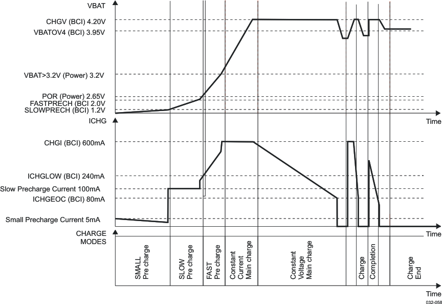 Figure 5-57 Automatic Charge Sequence Timing Diagram
5.5.5 CEA Charger Type
Depending on the device and according to the charger type, the DM and DP lines have different characteristics:
- Hub: DP and DM not shorted, DM low
- Charger: DP and DM shorted
- Carkit: DP and DM not shorted, DM high
These characteristics reflect to which of these devices the phone is connected.
Table 5-73 lists the important characteristics in precharge detection.
Table 5-73 Precharge Detection Characteristics
| Symbol | Parameter | Comments | Min | Max | Unit |
|---|---|---|---|---|---|
| ICCINIT | Supply current of unconfigured function/hub | Hub: DP and DM not shorted, DM low | 100 | mA | |
| ICRINIT | Supply current of unconfigured charger/carkit | Charger: DP and DM shorted Carkit: DP and DM not shorted, DM high |
100 | mA | |
| TDELAY | Delay for power up all blocks | 1000 | μs | ||
| TDMOD_DELAY | Time pulling down DM line | 19.5 | μs | ||
| TCHECK | Repeat time check process | 500 | ms | ||
| TPULSE | DP pullup pulse width | 20 | ms |
In main charge, the basic chargers and basic carkits indicate their default current limit, versus the value of the ID resistor, between the ID pin and the ground, and also versus the data bus D± connection type (shorted or not shorted).
Table 5-74 lists the output current limit ranges according to the device type and parameters.
Table 5-74 Main Charge Current Limit Indication
| Device Type | Parameter | Output Current Limit | ||||||
|---|---|---|---|---|---|---|---|---|
| ID Resistor (1%) | Output Voltage (nom) | D+/D– Connection(2) | ID Pin State |
ID Pin Current Limit Implemented | Min | Max | Unit | |
| Phone-powered accessory | 102k | N/A(1) | Not shorted | N/A | N/A | N/A | N/A | |
| Charger 5-wire | 200k | 5.0 V | Shorted | Low | N/A | 450 | 650 | mA |
| High | No | 450 | 650 | |||||
| High | Yes | 750 | 950 | |||||
| 440k | 5.0 V | Shorted | Low | N/A | 750 | 950 | mA | |
| High | No | 750 | 950 | |||||
| 4.5 V | Shorted | High | Yes | 1.8 | 3.0(3) | A | ||
| Basic carkit 5-wire | 200k | 5.0 V | D-high | Used for muting | N/A | 450 | 650 | mA |
| 440k | 5.0 V | D-high | Used for muting | N/A | 750 | 950 | ||
| Smart carkit 5-wire | N/A | 5.0 V | D-high | N/A | N/A | 0.450 | 3.0(3) | A |
| Carkit 4-wire | N/A | 5.0 V | D-high | N/A | N/A | 0.450 | 3.0(3) | A |
5.6 MADC
5.6.1 General Description
The TPS65950 shares the MADC resource with the host processors in the system (hardware and software conversion modes) and its BCI. Therefore, the TPS65950 must:
- Manage potential concurrent requests of conversions and priority among resource users
- Flag, using interrupt signals, the end-of-sequence of conversions
- Grant quarter-bit accuracy for modem conversion of battery voltage
The quarter-bit accurate start signal is provided through a STARTADC from the host processor (real-time conversion).
The MADC generates interrupt signals to the host processors. Interrupts are handled primarily by the MADC internal secondary interrupt handler (SIH) and secondly at the upper level (outside the MADC) by the TPS65950 primary interrupt handler (PIH). The MADC indicates to the BCI module, through a data ready signal, that conversion results are available.
5.6.2 Main Electrical Characteristics
Table 5-75 lists the electrical characteristics of the MADC.
Table 5-75 Electrical Characteristics
| Parameter | Conditions | Min | Typ | Max | Unit |
|---|---|---|---|---|---|
| Resolution | 10 | Bit | |||
| Input dynamic range for external input | Except ADIN0 and ADCIN1 and internal MADC input (0 to 1.5 V) | 0 | 2.5 | V | |
| MADC voltage reference | 1.5 | V | |||
| Differential nonlinearity | For all channels (except ADIN2 through ADIN7 channels) | –1 | 1 | LSB | |
| Integral nonlinearity | Best fitting. For all channels (except ADIN2 through ADIN7) | –2 | 2 | LSB | |
| Differential nonlinearity for ADIN2 through ADIN7 | –1 | 1 | LSB | ||
| Integral nonlinearity for ADIN2 through ADIN7 | Best fitting for codes 230 to maximum | –2 | 2 | LSB | |
| Best fitting considering offset of 25 least-significant bits (LSBs) | –3.75 | 3.75 | LSB | ||
| Offset | Best fitting | –28.5 | 28.5 | mV | |
| Input bias | 1 | μA | |||
| Input capacitor CBANK | 10 | pF | |||
| Maximum source input resistance Rs (for all 16 internal or external inputs) | 100 | kΩ | |||
| Input current leakage (for all 16 internal or external inputs) | 1 | μA |
5.6.3 Channel Voltage Input Range
Table 5-76 lists the channel voltage input ranges.
Table 5-76 Analog Input Voltage Range
| Channel | Min | Typ | Max | Unit | Prescaler |
|---|---|---|---|---|---|
| ADIN0: Battery type/GP input | 0 | 1.5 | V | No prescaler dc current source for battery identification through external resistor (10 μA typical) |
|
| ADCIN1: Battery temperature | 0 | 1.5 | V | No prescaler dc current source for temperature measurement through external resistor (10 to 80 μA programmable) |
|
| ADIN2: GP input(1) | 0 | 2.5 | V | MADC prescaler from 0 to >1.5 V | |
| ADIN3: GP input(1) | 0 | 2.5 | V | MADC prescaler from 0 to >1.5 V | |
| ADIN4: GP input(1) | 0 | 2.5 | V | MADC prescaler from 0 to >1.5 V | |
| ADIN5: GP input(1) | 0 | 2.5 | V | MADC prescaler from 0 to >1.5 V | |
| ADIN6: GP input(1) | 0 | 2.5 | V | MADC prescaler from 0 to >1.5 V | |
| ADIN7: GP input(1) | 0 | 2.5 | V | MADC prescaler from 0 to >1.5 V |
5.6.3.1 Sequence Conversion Time (Real-Time or Nonaborted Asynchronous)
Table 5-77 lists the sequence conversion timing characteristics. Figure 5-58 is a conversion sequence general timing diagram.
Table 5-77 Sequence Conversion Timing Characteristics
| Parameter | Comments | Min | Typ | Max | Unit |
|---|---|---|---|---|---|
| F | Running frequency | 1 | MHz | ||
| T = 1/F | Clock period | 1 | μs | ||
| N | Number of analog inputs to convert in a single sequence | 0 | 16 | ||
| Tstart | SW1, SW2, or USB asynchronous request or real-time STARTADC request | 3 | 4 | μs | |
| Tsettling time | Settling time to wait before sampling a stable analog input (capacitor bank charge time) | 5 | 12 | 20 | μs |
| Tsettling is calculated from the max ((Rs + Ron)*Cbank) of the 16 possible input sources (internal or external). Ron is the resistance of the selection analog input switches (5 kΩ). This time is software-programmable in the open-core protocol (OCP) register. | |||||
| Tstartsar | The successive approximation registers ADC start time. | 1 | μs | ||
| Tadc time | The successive approximation registers ADC conversion time. | 10 | μs | ||
| Tcapture time | Tcapture time is the conversion result capture time. | 2 | μs | ||
| Tstop | 1 | 2 | μs | ||
| Full conversion sequence time | One channel (N = 1)(1) | 22 | 39 | μs | |
| All channels (N = 16)(1) | 352 | 624 | |||
| Conversion sequence time | Without Tstart and Tstop: One channel (N = 1)(1) | 18 | 33 | μs | |
| Without Tstart and Tstop: All channels (N = 16)(1) | 288 | 528 | |||
| STARTADC pulse duration | STARTADC period is T | 0.33 | 24 | μs |
Table 5-77 shows the information in Figure 5-58. The Busy parameter shows that a conversion sequence is running, and the channel N result register parameter corresponds to the result register of RT/GP/BCI selected channel.
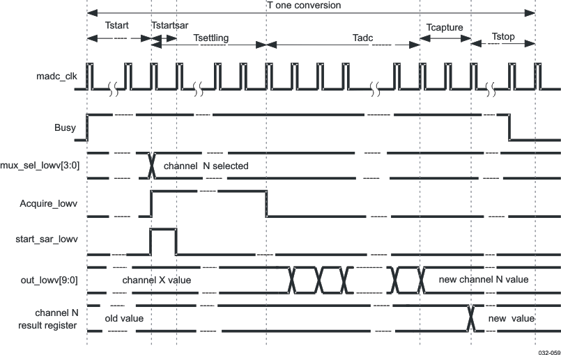 Figure 5-58 Conversion Sequence General Timing Diagram
5.7 LED Drivers
5.7.1 General Description
Two arrays of parallel LEDs are driven (dedicated for the phone light). The parallel LEDs are supplied by VBAT and the external resistor value is given for each of them. The TPS65950 has two open-drain LED drivers for keypad backlighting. The keypad backlighting must incorporate any required current limiting and be rated for operation at the main battery voltage.
Figure 5-59 is a block diagram of the LED driver. Table 5-78 lists the electrical characteristics of the LED driver.
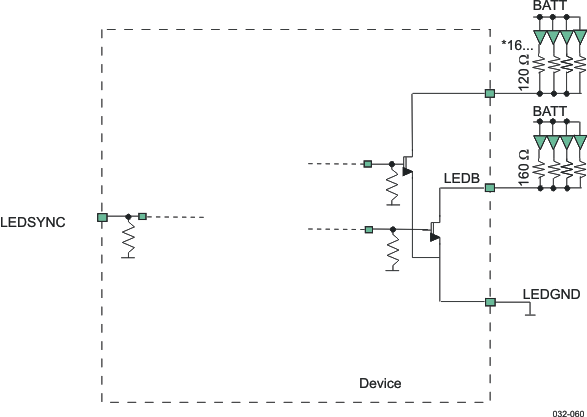 Figure 5-59 LED Driver Block Diagram
For the component values, see Table 5-92.
Table 5-78 Electrical Characteristics
| Parameter | Conditions | Min | Typ | Max | Unit |
|---|---|---|---|---|---|
| Software On resistance | IO = 160 mA | 3 | 4 | Ω | |
| IO = 60 mA | 10 | 12 |
5.8 Keyboard
5.8.1 Keyboard Connection
The keyboard is connected to the chip using:
- KBR (7:0) input pins for row lines
- KBC (7:0) output pins for column lines
Figure 5-60 shows the keyboard connection.
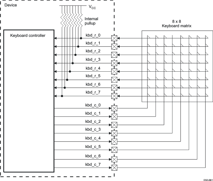 Figure 5-60 Keyboard Connection
When a key button of the keyboard matrix is pressed, the corresponding row and column lines are shorted together. To allow key press detection, all input pins (KBR) are pulled up to VCC and all output pins (KBC) are driven low.
Any action on a button generates an interrupt to the sequencer.
The decoding sequence is written to allow detection of simultaneous press actions on several key buttons.
The keyboard interface can be used with a smaller keyboard area than 8 × 8. To use a 6 × 6 keyboard, KBR(6) and KBR(7) must be tied high to prevent any scanning process distribution.
5.9 Clock Specifications
The TPS65950 includes several I/O clock pins. The TPS65950 has two sources of high-stability clock signals: the external high-frequency clock (HFCLKIN) input and an onboard 32-kHz oscillator (an external 32-kHz signal can be provided). Figure 5-61 is an overview of the clocks.
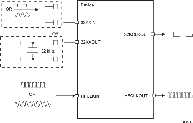 Figure 5-61 Clock Overview
5.9.1 Features
The TPS65950 accepts two sources of high-stability clock signals:
- 32KXIN/32KXOUT: Onboard 32-kHz crystal oscillator (an external 32-kHz input clock can be provided)
- HFCLKIN: External high-frequency clock (19.2, 26, or 38.4 MHz).
The TPS65950 can provide:
- 32KCLKOUT digital output clock
- HFCLKOUT digital output clock with the same frequency as the HFCLKIN input clock
5.9.2 Input Clock Specifications
The clock system accepts two input clock sources:
- 32-kHz crystal oscillator clock or sinusoidal/squared clock
- HFCLKIN high-frequency input clock
5.9.2.1 Clock Source Requirements
Table 5-79 lists the input clock requirements.
Table 5-79 TPS65950 Input Clock Source Requirements
| Pad | Clock Frequency | Stability | Duty Cycle | |
|---|---|---|---|---|
| 32KXIN 32KXOUT |
32.768 kHz | Crystal | ±30 ppm | 40%/60% |
| Square wave | – | 45%/55% | ||
| Sine wave | – | – | ||
| HFCLKIN | 19.2, 26, 38.4 MHz | Square wave | ±150 ppm | See (1) |
| Sine wave | – | – | ||
5.9.2.2 High-Frequency Input Clock
HFCLKIN is the high-frequency input clock. It can be a square- or sine-wave input clock. If a square-wave input clock is provided, it is recommended to switch the block to bypass mode when possible to avoid loading the clock.
Figure 5-62 shows the HFCLKIN clock distribution.
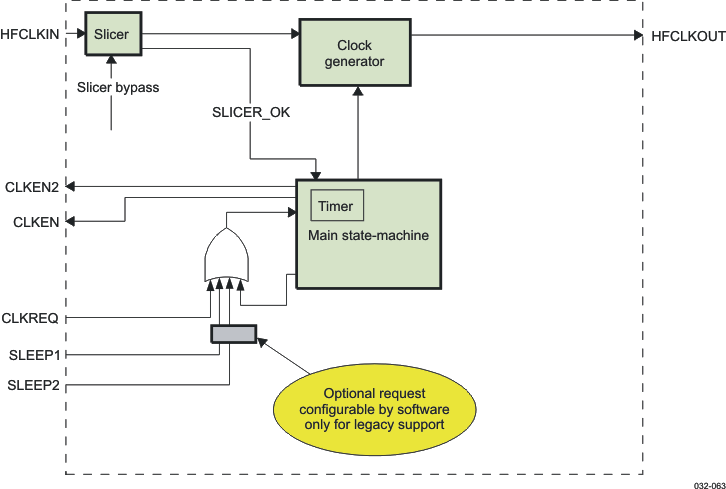 Figure 5-62 HFCLKIN Clock Distribution
When a device needs a clock signal other than 32.768 kHz, it makes a clock request and activates the CLKREQ pin. As a result, the TPS65950 immediately sets CLKEN to 1 to warn the clock provider in the system about the clock request and starts a timer (maximum of 5.2 ms using the 32.768-kHz clock). When the timer expires, the TPS65950 opens a gated clock, the timer automatically reloads the defined value, and a high-frequency output clock signal is available through the HFCLKOUT pin. The output drive of HFCLKOUT is programmable (minimum load 10 pF, maximum load 40 pF) and must be at 40 pF by default.
With a register setting, the mirroring of CLKEN can be enabled on CLKEN2. When this mirroring feature is not enabled, CLKEN2 can be used as a GP output controlled through I2C accesses.
CLKREQ, when enabled, has a weak pulldown resistor to support the wired-OR clock request.
Figure 5-63 shows an example of the wired-OR clock request.
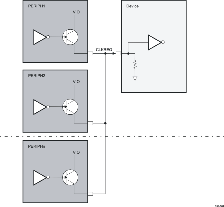 Figure 5-63 Example of Wired-OR Clock Request
NOTE
The timer default value must be the worst case (10 ms) for the clock providers. For legacy or workaround support, the signals NSLEEP1 and NSLEEP2 can also be used as a clock request even if it is not their primary goal. By default, this feature is disabled and must be enabled individually by setting the register bits associated with each signal.
When the external clock signal is present on the HFCLKIN ball, it is possible to use this clock instead of the internal RC oscillator and then synchronize the system on the same clock. The RC oscillator can then go to idle mode.
Table 5-80 lists the input clock electrical characteristics of the HFCLKIN input clock.
Table 5-80 HFCLKIN Input Clock Electrical Characteristics
| Parameter | Configuration Mode Slicer | Min | Typ | Max | Unit |
|---|---|---|---|---|---|
| Frequency | 19, 26, or 38.4 | MHz | |||
| Startup time | LP/HP (sine wave) | 4 | μs | ||
| Input dynamic range | LP/HP (sine wave) | 0.3 | 0.7 | 1.45 | VPP |
| BP/PD (square wave) | 0 | 1.85(1) | |||
| Current consumption | LP | 175 | μA | ||
| HP | 235 | ||||
| BP/PD | 39 | nA | |||
| Harmonic content of input signal (with 0.7-VPP amplitude): second component | LP/HP (sine wave) | –25 | dBc | ||
| Voltage input high (VIH) | BP (square wave) | 1 | V | ||
| Voltage input low (VIL) | BP (square wave) | 0.6 | V | ||
Table 5-81 lists the input clock timing requirements of the HFCLKIN input clock when the source is a square wave.
Table 5-81 HFCLKIN Square Input Clock Timing Requirements With Slicer in Bypass
| Name | Parameter | Description | Min | Typ | Max | Unit |
|---|---|---|---|---|---|---|
| CH0 | 1/tC(HFCLKIN) | Frequency, HFCLKIN | 19.2, 26, or 38.4 | MHz | ||
| CH1 | tW(HFCLKIN) | Pulse duration, HFCLKIN low or high | 0.45*tC(HFCLKIN) | 0.55*tC(HFCLKIN) | ns | |
| CH3 | tR(HFCLKIN) | Rise time, HFCLKIN(1) | 5 | ns | ||
| CH4 | tF(HFCLKIN) | Fall time, HFCLKIN(1) | 5 | ns | ||
Figure 5-64 shows the timing of the HFCLKIN squared input clock.
 Figure 5-64 HFCLKIN Squared Input Clock
5.9.2.3 32-kHz Input Clock
A 32.768-kHz input clock (often abbreviated to 32-kHz) generates the clocks for the RTC. It has a low-jitter mode where the current consumption increases for lower jitter. It is possible to use the 32-kHz input clock with an external crystal or clock source. Depending on the mode, the 32K oscillator is configured as being either:
- An external 32.768-kHz crystal through the 32KXIN/32KXOUT balls (see Figure 5-65). This configuration is available for master mode only (for more information, see Section 4.7, Timing Requirements and Switching Characteristics).
- An external square or sine wave of 32.768 kHz through 32KXIN with amplitude of 1.8 or 1.85 V (see Figure 5-67, Figure 5-68, and Figure 5-69). This configuration is available for master and slave modes (for more information, see Section 4.7, Timing Requirements and Switching Characteristics).
5.9.2.3.1 External Crystal Description
Figure 5-65 is a block diagram of the 32-kHz oscillator with crystal in master mode.
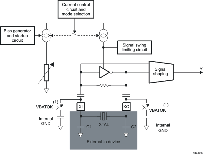
CXIN and CXOUT represent the total capacitance of the printed circuit board (PCB) and components, excluding the crystal. Their values depend on the datasheet of the crystal, the internal capacitors, and the parallel capacitor. The frequency of the oscillations depends on the value of the capacitors. The crystal must be in the fundamental mode of operation and parallel resonant.
NOTE
For the values of CXIN and CXOUT, see Table 5-92.
Table 5-82 lists the required electrical constraints.
Table 5-82 Crystal Electrical Characteristics
| Parameter | Min | Typ | Max | Unit |
|---|---|---|---|---|
| Parallel resonance crystal frequency | 32.768 | kHz | ||
| Input voltage, Vin (normal mode) | 1.0 | 1.3 | 1.55 | V |
| Internal capacitor on each input (Cint) | 10 | pF | ||
| Parallel input capacitance (Cpin) | 1 | pF | ||
| Nominal load cap on each oscillator input CXIN and CXOUT(1) | CXIN = CXOUT = Cosc*2 – (Cint + Cpin) | pF | ||
| Pin-to-pin capacitance | 1.6 | 1.8 | pF | |
| Crystal ESR(2) | 75 | kΩ | ||
| Crystal shunt capacitance, CO | 1 | pF | ||
| Crystal tolerance at room temperature, 25°C | –30 | 30 | ppm | |
| Crystal tolerance versus temperature range (–40°C to 85°C) | –200 | 200 | ppm | |
| Maximum drive power | 1 | μW | ||
| Operating drive level | 0.5 | μW | ||
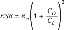
Measured with the load capacitance specified by the crystal manufacturer. If CXIN = CXOUT = 10 pF, then CL = 5 pF. Parasitic capacitance from the package and board must also be considered.
When selecting a crystal, the system design must consider the temperature and aging characteristics of a crystal versus the user environment and expected lifetime of the system.
Table 5-83 and Table 5-84 list the switching characteristics of the oscillator and the input requirements of the 32.768-kHz input clock, respectively. Figure 5-66 shows the crystal oscillator output in normal mode.
Table 5-83 Base Oscillator Switching Characteristics
| Name | Parameter Description | Min | Typ | Max | Unit | |
|---|---|---|---|---|---|---|
| fP | Oscillation frequency | 32.768 | kHz | |||
| tSX | Startup time | 0.5 | s | |||
| IDDA | Active current consumption | LOJIT <1:0> = 00 | 1.8 | μA | ||
| LOJIT <1:0> = 11 | 8 | |||||
| IDDQ | Current consumption | Low battery mode (1.2 V) | 1 | μA | ||
| Startup | 8 | |||||
Table 5-84 32-kHz Crystal Input Clock Timing Requirements
| Name | Parameter Description | Min | Typ | Max | Unit | |
|---|---|---|---|---|---|---|
| OC0 | 1/tC(32KHZ) | Frequency, 32 kHz | 32.768 | kHz | ||
| OC1 | tW(32KHZ) | Pulse duration, 32 kHz low or high | 0.40*tC(32KHZ) | 0.60*tC(32KHZ) | μs | |
 Figure 5-66 32-kHz Crystal Input
5.9.2.3.2 External Clock Description
Figure 5-67 and Figure 5-68 show the 32-kHz oscillator with a 32.768-kHz square or sine signal in master and slave modes. Figure 5-69 shows an external clock source when the oscillator is configured in bypass mode. Thus, there are three configurations:
- A square- or sine-wave input can be applied to the 32KXIN pin with an amplitude of 1.85 or 1.8 V. The 32KXOUT pin can be driven to a dc value of the square- or sine-wave amplitude divided by 2. This configuration, shown in Figure 5-67, is recommended if a large load is applied on the 32KXOUT pin.
- A square- or sine-wave input can be applied to the 32KXIN pin with an amplitude of 1.85 or 1.8 V. The 32KXOUT pin can be left floating. This configuration, showed in Figure 5-68, is used if no charge is applied on the 32KXOUT pin.
- The oscillator is in bypass mode and a square-wave input can be applied to the 32KXIN pin with an amplitude of 1.8 V. The 32KXOUT pin can be left floating. This configuration, shown in Figure 5-69, is used if the oscillator is in bypass mode.
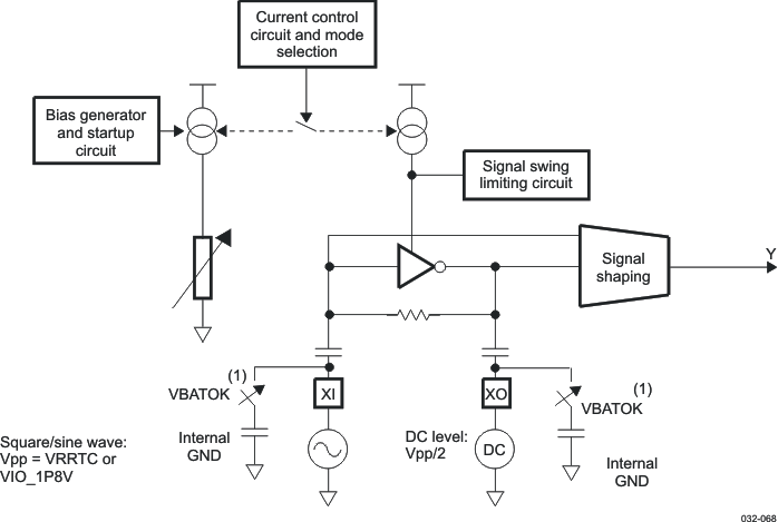

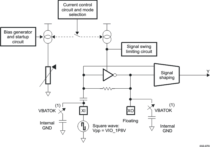
Table 5-85 lists the electrical constraints required by the 32-kHz input square- or sine-wave clock used.
Table 5-85 32-kHz Input Square- or Sine-Wave Clock Source Electrical Characteristics
| Name | Parameter Description | Min | Typ | Max | Unit |
|---|---|---|---|---|---|
| f | Frequency | 32.768 | kHz | ||
| CI | Input capacitance | 35 | pF | ||
| CFI | On-chip foot capacitance to GND on each input (see Figure 5-67, Figure 5-68, and Figure 5-69) | 10 | pF | ||
| VPP | Square-/sine-wave amplitude in bypass mode or not | 1.8(1) | V | ||
| VIH | Voltage input high, square wave in bypass mode | 0.8 | V | ||
| VIL | Voltage input low, square wave in bypass mode | 0.6 | V | ||
Table 5-86 lists the input requirements of the 32-kHz square-wave input clock.
Table 5-86 32-kHz Square-Wave Input Clock Source Timing Requirements
| Name | Parameter | Description | Min | Typ | Max | Unit |
|---|---|---|---|---|---|---|
| CK0 | 1/tC(32KHZ) | Frequency, 32 kHz | 32.768 | MHz | ||
| CK1 | tW(32KHZ) | Pulse duration, 32 kHz low or high | 0.45*tC(32KHZ) | 0.55*tC(32KHZ) | μs | |
| CK3 | tR(32KHZ) | Rise time, 32 kHz(1) | 0.1*tC(32KHZ) | μs | ||
| CK4 | tF(32KHZ) | Fall time, 32 kHz(1) | 0.1*tC(32KHZ) | μs | ||
Figure 5-70 shows the timing of the 32-kHz square- or sine-wave input clock.
 Figure 5-70 32-kHz Square- or Sine-Wave Input Clock
5.9.3 Output Clock Specifications
The TPS65950 provides two output clocks:
- 32KCLKOUT
- HFCLKOUT
5.9.3.1 32KCLKOUT Output Clock
Figure 5-71 is a block diagram of the 32.768-kHz clock output.
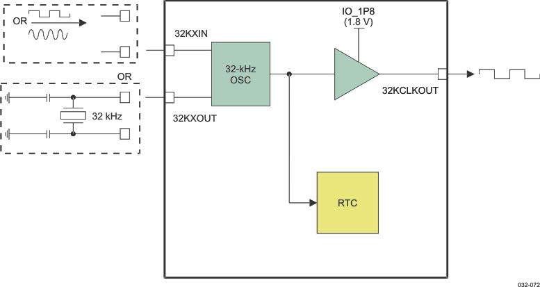 Figure 5-71 32.768-kHz Clock Output Block Diagram
The TPS65950 has an internal 32.768-kHz oscillator connected to an external 32.768-kHz crystal through the 32KXIN/32KXOUT balls or an external digital 32.768-kHz clock through the 32KXIN input (see Figure 5-71). The TPS65950 also generates a 32.768-kHz digital clock through the 32KCLKOUT pin and can broadcast it externally to the application processor or any other devices. The 32KCLKOUT clock is broadcast by default in the TPS65950 active mode, but can be disabled if it is not used.
The 32.768-kHz clock (or signal) also clocks the RTC embedded in the TPS65950. The RTC is not enabled by default. The host processor must set the correct date and time and enable the RTC.
The 32KCLKOUT output buffer can drive several devices (up to a 40-pF load). At startup, the 32.768-kHz output clock (32KCLKOUT) must be stabilized (frequency/duty cycle) before the signal output. Depending on the startup condition, this can delay the startup sequence.
Table 5-87 lists the electrical characteristics of the 32KCLKOUT output clock.
Table 5-87 32KCLKOUT Output Clock Electrical Characteristics
| Name | Parameter Description | Min | Typ | Max | Unit |
|---|---|---|---|---|---|
| f | Frequency | 32.768 | kHz | ||
| CL | Load capacitance | 40 | pF | ||
| VOUT | Output clock voltage, depending on output reference level IO_1P8 (see Section 3) | 1.8(1) | V | ||
| VOH | Voltage output high | VOUT – 0.45 | VOUT | V | |
| VOL | Voltage output low | 0 | 0.45 | V |
Table 5-88 lists the timing characteristics of the 32KCLKOUT output clock. Figure 5-72 shows the waveform of the 32KCLKOUT output clock.
Table 5-88 32KCLKOUT Output Clock Switching Characteristics
| Name | Parameter | Description | Min | Typ | Max | Unit |
|---|---|---|---|---|---|---|
| CK0 | 1/tC(32KCLKOUT) | Frequency | 32.768 | MHz | ||
| CK1 | tW(32KCLKOUT) | Pulse duration, 32KCLKOUT low or high | 0.40*tC(32KCLKOUT) | 0.60*tC(32KCLKOUT) | ns | |
| CK2 | tR(32KCLKOUT) | Rise time, 32KCLKOUT(1) | 16 | ns | ||
| CK3 | tF(32KCLKOUT) | Fall time, 32KCLKOUT(1) | 16 | ns |
 Figure 5-72 32KCLKOUT Output Clock
5.9.3.2 HFCLKOUT Output Clock
Table 5-89 lists the electrical characteristics of the HFCLKOUT output clock.
Table 5-89 HFCLKOUT Output Clock Electrical Characteristics
| Name | Parameter Description | Min | Typ | Max | Unit |
|---|---|---|---|---|---|
| f | Frequency | 19.2, 26, or 38.4 | MHz | ||
| CL | Load capacitance | 30 | pF | ||
| VOUT | Output clock voltage, depending on output reference level IO_1P8 (see Section 3) | 1.8(1) | V | ||
| VOH | Voltage output high | VOUT – 0.45 | VOUT | V | |
| VOL | Voltage output low | 0 | 0.45 | V | |
Table 5-90 lists the timing characteristics of the HFCLKOUT output clock.
Table 5-90 HFCLKOUT Output Clock Switching Characteristics
| Name | Parameter | Description | Min | Typ | Max | Unit |
|---|---|---|---|---|---|---|
| CHO1 | 1/tC(HFCLKOUT) | Frequency | 19.2, 26, or 38.4 | MHz | ||
| CHO2 | tW(HFCLKOUT) | Pulse duration, HFCLKOUT low or high | 0.40*tC(HFCLKOUT) | 0.60*tC(HFCLKOUT) | ns | |
| CHO3 | tR(HFCLKOUT) | Rise time, HFCLKOUT(1) | 2.6 | ns | ||
| CHO4 | tF(HFCLKOUT) | Fall time, HFCLKOUT(1) | 2.6 | ns | ||
Figure 5-73 shows the waveform of the HFCLKOUT output clock.
 Figure 5-73 HFCLKOUT Output Clock
5.9.3.3 Output Clock Stabilization Time
Figure 5-74 shows the 32KCLKOUT and HFCLKOUT clock stabilization time.
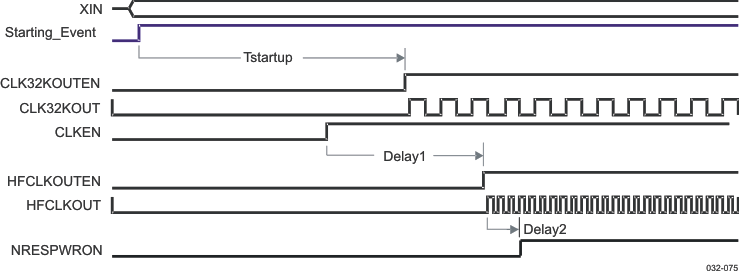
Figure 5-75 shows the behavior of HFLCKOUT.
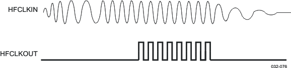 Figure 5-75 HFCLKOUT Behavior
5.10 Debouncing Time
Table 5-91 lists the debouncing functions.
Table 5-91 Debouncing Time
| Debouncing Functions | Block | Programmable | Debouncing Time | Default |
|---|---|---|---|---|
| Main battery charged threshold (<3.2 V) | Battery monitoring | No | 580 μs | 580 μs |
| Main battery low threshold detection (<2.7 V) | No | 60 μs | 60 μs | |
| Main battery plug detection (with charger connected) | No | 60 μs | 60 μs | |
| Charger unplug detection(1) | BCI (automatic charge) |
No | 1 x 50 ms | 1 x 50 ms |
| Charger plug detection(1) | BCI | No | 9 x 50 ms | 9 x 50 ms |
| Debouncing functions interrupt generation debounce for charger plug | Power | No | 125.6 μs | 125.6 μs |
| USB plug detection/VBUS precharge (same debouncing as charger plug) (1) | BCI | No | 9 x 50 ms | 9 x 50 ms |
| Battery presence plug/unplug(1) | BCI | No | 9 x 50 ms | 9 x 50 ms |
| Battery thermistor in/out of range (1) | BCI | No | 4 x 50 ms | 4 x 50 ms |
| Plug/unplug detection VBUS(2) | USB | Yes | 0 to 250 ms (32/32,468-second steps) |
28 ms |
| Plug/unplug detection ID(3) | USB | Yes | 0 to 250 ms (32/32,468-second steps) |
50 ms |
| Debouncing functions interrupt generation debounce for VBUS and ID(4) | Power | Yes | 0 to 250 ms | 30 ms |
| Hot-die detection | Thermistor | No | 60 μs | 60 μs |
| Thermal shutdown detection | No | 60 μs | 60 μs | |
| PWRON(5) | Start/stop button | No | 31.25 ms | 31.25 ms |
| NRESWARM | Button reset | No | 60 μs | 60 μs |
| SIM card plug/unplug | GPIO | Yes | 0 or 30 ms ± 1 ms | 0 ms |
| Headset detection (plug/unplug) | GPIO | Yes | 0 or 30 ms ± 1 ms | 0 ms |
| MMC1/2 (plug/unplug) | GPIO | Yes | 0 or 30 ms ± 1 ms | 0 ms |
 Figure 5-76 Debouncing Sequence Chronogram Example
Event 1 is correctly debounced after 50 ms. Event 2 is debounced after 50 ms + dT because the capture of the event is considered after the next rising edge of the 50-ms clock.
5.11 External Components
Table 5-92 lists the external components of the TPS65950.
Table 5-92 TPS65950 External Components
| Function | Component | Reference | Value | Note | Link |
|---|---|---|---|---|---|
| Power Supplies | |||||
| VDD1 | Capacitor | CVDD1.IN | 10 μF | Range ± 50% ESR minimum = 1 mΩ ESR maximum = 20 mΩ Taiyo Yuden: JMK212BJ106KD |
Figure 5-1 |
| Capacitor | CVDD1.OUT | 10 μF | Range ± 50% ESR minimum = 1 mΩ ESR maximum = 20 mΩ Taiyo Yuden: JMK212BJ106KD |
||
| Inductor | LVDD1 | 1 μH | Range ± 30% DCR maximum = 100 mΩ |
||
| VDD2 | Capacitor | CVDD2.IN | 10 μF | Range ± 50% ESR minimum = 1 mΩ ESR maximum = 20 mΩ Taiyo Yuden: JMK212BJ106KD |
Figure 5-1 |
| Capacitor | CVDD2.OUT | 10 μF | Range ± 50% ESR minimum = 1 mΩ ESR maximum = 20 mΩ Taiyo Yuden: JMK212BJ106KD |
||
| Inductor | LVDD2 | 1 μH | Range ± 30% DCR maximum = 100 mΩ |
||
| VIO | Capacitor | CVIO.IN | 10 μF | Range ± 50% ESR minimum = 1 mΩ ESR maximum = 20 mΩ Taiyo Yuden: JMK212BJ106KD |
Figure 5-1 |
| Capacitor | CVIO.OUT | 10 μF | Range ± 50% ESR minimum = 1 mΩ ESR maximum = 20 mΩ Taiyo Yuden: JMK212BJ106KD |
||
| Inductor | LVVIO | 1 μH | Range ± 30% DCR maximum = 100 mΩ |
||
| VRUSB_3V | Capacitor | CVUSB.3P1 | 1 μF | Range: 0.3 to 2.7 μF ESR minimum = 20 mΩ ESR maximum = 300 mΩ |
Figure 5-1Figure 5-48 |
| VRUSB_1V5 | Capacitor | CVINTUSB1P5.OUT | 1 μF | Range: 0.3 to 2.7 μF ESR minimum = 20 mΩ ESR maximum = 600 mΩ |
Figure 5-1Figure 5-48 |
| VRUSB_1V8 | Capacitor | CVINTUSB1P8.OUT | 1 μF | Range: 0.3 to 2.7 μF ESR minimum = 20 mΩ ESR maximum = 600 mΩ |
Figure 5-1Figure 5-48 |
| VDAC | Capacitor | CVDAC.IN | 1 μF | Range: 0.3 to 2.7 μF ESR minimum = 20 mΩ ESR maximum = 600 mΩ |
Figure 5-1 |
| Capacitor | CVDAC.OUT | 1 μF | Range: 0.3 to 2.7 μF ESR minimum = 20 mΩ ESR maximum = 600 mΩ |
||
| VPLLA3R | Capacitor | CVPLLA3R.IN | 1 μF | Range: 0.3 to 2.7 μF ESR minimum = 20 mΩ ESR maximum = 600 mΩ |
Figure 5-1 |
| VPLL1 | Capacitor | CVPLL1.OUT | 1 μF | Range: 0.3 to 2.7 μF ESR minimum = 20 mΩ ESR maximum = 600 mΩ |
Figure 5-1 |
| VPLL2/VDSI.CSI | Capacitor | CVPLL2.OUT | 1 μF | Range: 0.3 to 2.7 μF ESR minimum = 20 mΩ ESR maximum = 600 mΩ |
Figure 5-1 |
| VMMC1 | Capacitor | CVMMC1.IN | 1 μF | Range: 0.3 to 2.7 μF ESR minimum = 20 mΩ ESR maximum = 600 mΩ |
Figure 5-1 |
| Capacitor | CVMMC1.OUT | 1 μF | Range: 0.3 to 2.7 μF ESR minimum = 20 mΩ ESR maximum = 600 mΩ |
||
| VMMC2 | Capacitor | CVMMC2.IN | 1 μF | Range: 0.3 to 2.7 μF ESR minimum = 20 mΩ ESR maximum = 600 mΩ |
Figure 5-1 |
| Capacitor | CVMMC2.OUT | 1 μF | Range: 0.3 to 2.7 μF ESR minimum = 20 mΩ ESR maximum = 600 mΩ |
||
| VSIM | Capacitor | CVSIM.OUT | 1 μF | Range: 0.3 to 2.7 μF ESR minimum = 20 mΩ ESR maximum = 600 mΩ |
Figure 5-1 |
| VAUX12S | Capacitor | CVAUX12S.IN | 1 μF | Range: 0.3 to 2.7 μF ESR minimum = 20 mΩ ESR maximum = 600 mΩ |
Figure 5-1 |
| VAUX1 | Capacitor | CVAUX1.OUT | 1 μF | Range: 0.3 to 2.7 μF ESR minimum = 20 mΩ ESR maximum = 600 mΩ |
Figure 5-1 |
| VAUX2 | Capacitor | CVAUX2.OUT | 1 μF | Range: 0.3 to 2.7 μF ESR minimum = 20 mΩ ESR maximum = 600 mΩ |
Figure 5-1 |
| VAUX3 | Capacitor | CVAUX3.OUT | 1 μF | Range: 0.3 to 2.7 μF ESR minimum = 20 mΩ ESR maximum = 600 mΩ |
Figure 5-1 |
| VAUX4 | Capacitor | CVAUX4.IN | 1 μF | Range: 0.3 to 2.7 μF ESR minimum = 20 mΩ ESR maximum = 600 mΩ |
Figure 5-1 |
| Capacitor | CVAUX4.OUT | 1 μF | Range: 0.3 to 2.7 μF ESR minimum = 20 mΩ ESR maximum = 600 mΩ |
||
| VINT | Capacitor | CVINT.IN | 1 μF | Range: 0.3 to 2.7 μF ESR minimum = 20 mΩ ESR maximum = 600 mΩ |
Figure 5-1 |
| VINTANA1 | Capacitor | CVINTANA1.OUT | 1 μF | Range: 0.3 to 2.7 μF ESR minimum = 20 mΩ ESR maximum = 600 mΩ |
Figure 5-1 |
| VINTANA2 | Capacitor | CVINTANA2.OUT | 1 μF | Range: 0.3 to 2.7 μF ESR minimum = 20 mΩ ESR maximum = 600 mΩ |
Figure 5-1 |
| VINTDIG | Capacitor | CVINTDIG.OUT | 1 μF | Range: 0.3 to 2.7 μF ESR minimum = 20 mΩ ESR maximum = 600 mΩ |
Figure 5-1 |
| VBAT.USB | Capacitor | CVBAT.USB | 1 μF | Range: 0.3 to 2.7 μF ESR minimum = 20 mΩ ESR maximum = 600 mΩ |
Figure 5-48 |
| USB CP | Capacitor | CVBUS.FC | 2.2 μF ±40% | ESR maximum = 20 mΩ | Figure 5-48 |
| Capacitor | CVBUS.IN | 10 μF | |||
| Capacitor | CVBUS | 4.7 μF ±40% | ESR maximum = 20 mΩ | ||
| MCPC | |||||
| Capacitor | CTXAF | 0.1 μF | Figure 5-48 | ||
| Capacitor | CRXAF | 1 μF | |||
| Resistor | RRTSO | 22 Ω/100 Ω | |||
| Diode | DCTSI1 | NNCD5.6J | |||
| Diode | DCTSI2 | NNCD5.6J | |||
| Diode | DRTSO1 | NNCD5.6J | |||
| Diode | DRTSO2 | NNCD5.6J | |||
| 32.768 kHz | |||||
| Capacitor | CXIN | 10 pF | Range: 9 to 12.5 pF | Figure 5-65 | |
| Capacitor | CXOUT | 10 pF | |||
| Quartz | X32.768kHz | 32.768 kHz | ±30 ppm (at 25°C) ±200 ppm (–40°C to 85°C) |
||
| Audio | |||||
| Earpiece | Capacitor | CEAR | 100 pF | Figure 5-15 | |
| 8-Ω hands-free right | Ferrite bead | LHFR.M | NEC: N2012ZPS121 | Figure 5-17 | |
| Ferrite bead | LHFR.P | NEC: N2012ZPS121 | |||
| Capacitor | CHFR | 1 μF | |||
| Capacitor | CHFR.M | 1 nF | |||
| Capacitor | CHFR.P | 1 nF | |||
| 8-Ω hands-free left | Ferrite bead | LHFL.M | NEC: N2012ZPS121 | Figure 5-17 | |
| Ferrite bead | LHFL.P | NEC: N2012ZPS121 | |||
| Capacitor | CHFL | 1 μF | |||
| Capacitor | CHFL.M | 1 nF | |||
| Capacitor | CHFL.P | 1 nF | |||
| Headset left | Capacitor | CS | 22 μF/47 μF | Figure 5-19 through Figure 5-22 | |
| Resistor | RS | 0 to 33 Ω | |||
| Capacitor | CI | 47 pF | |||
| Headset right | Capacitor | CS | 22 μF/47 μF | Figure 5-19 through Figure 5-22 | |
| Resistor | RS | 0 to 33 Ω | |||
| Capacitor | CI | 47 pF | |||
| Headset microphone | Capacitor | CHM.M | 100 nF | Figure 5-19 through Figure 5-22 | |
| Capacitor | CHM.P | 100 nF | |||
| Capacitor | CHM.O | 47 pF | |||
| Resistor | RB + RSB | 2.2 kΩ/2.7 kΩ | |||
| Capacitor | CB | 0 to 200 pF | If greater than 200 pF, a serial resistor is required for bias stability. | ||
| External class-D predriver left | Capacitor | CPL.O | 50 pF | Figure 5-24 | |
| Capacitor | CPL | 1 μF | |||
| Resistor | RPL | >15 kΩ | |||
| Resistor | RPL.M | >15 kΩ | |||
| Resistor | RPL.O | 10 kΩ | |||
| Capacitor | CPL.M | 1 μF | |||
| External class-D predriver right | Capacitor | CPR.O | 50 pF | Figure 5-24 | |
| Capacitor | CPR | 1 μF | |||
| Resistor | RPR | >15 kΩ | |||
| Resistor | RPR.M | >15 kΩ | |||
| Resistor | RPR.O | 10 kΩ | |||
| Capacitor | CPR.M | 1 μF | |||
| Vibrator H-bridge | Ferrite bead | LV.M | BLM18BD221S1N | Figure 5-25 | |
| Ferrite bead | LV.P | BLM18BD221S1N | |||
| Capacitor | CV.V | 1 μF | |||
| Capacitor | CV.M | 1 nF | |||
| Capacitor | CV.P | 1 nF | |||
| Main microphone (pseudodifferential mode) | Capacitor | CMM.M | 100 nF | Figure 5-32 | |
| Capacitor | CMM.P | 100 nF | |||
| Capacitor | CMM.O | 47 pF | |||
| Resistor | RMM.O | ~500 Ω | |||
| Resistor | RMM.MP | ~1.7 kΩ | |||
| Capacitor | CMM.B | 0 to 200 pF | If greater than 200 pF, a serial resistor is required for bias stability. | ||
| Submicrophone (pseudodifferential mode) | Capacitor | CMS.M | 100 nF | Figure 5-32 | |
| Capacitor | CMS.P | 100 nF | |||
| Capacitor | CMS.O | 47 pF | |||
| Resistor | RMS.O | ~500 Ω | |||
| Resistor | RMS.MP | ~1.7 kΩ | |||
| Capacitor | CMS.B | 0 to 200 pF | If greater than 200 pF, a serial resistor is required for bias stability. | ||
| Main microphone (differential mode) | Capacitor | CMM.M | 100 nF | Figure 5-33 | |
| Capacitor | CMM.P | 100 nF | |||
| Capacitor | CMM.PM | 47 pF | |||
| Capacitor | CMM.O | 47 pF | |||
| Capacitor | CMM.GM | 47 pF | |||
| Capacitor | CMM.GP | 47 pF | |||
| Resistor | RMM.BP | 1 kΩ | |||
| Resistor | RMM.GM | 1 kΩ | |||
| Capacitor | CMM.B | 0 to 200 pF | If greater than 200 pF, a serial resistor is required for bias stability. | ||
| Submicrophone (differential mode) | Capacitor | CMS.M | 100 nF | Figure 5-33 | |
| Capacitor | CMS.P | 100 nF | |||
| Capacitor | CMS.PM | 47 pF | |||
| Capacitor | CMS.O | 47 pF | |||
| Capacitor | CMS.GM | 47 pF | |||
| Capacitor | CMS.GP | 47 pF | |||
| Resistor | RMS.BP | 1 kΩ | |||
| Resistor | RMS.GM | 1 kΩ | |||
| Capacitor | CMS.B | 0 to 200 pF | If greater than 200 pF, a serial resistor is required for bias stability. | ||
| VMIC1 | Capacitor | CVMIC1.OUT | 1 μF | Range: 0.3 to 3.3 μF ESR minimum = 20 mΩ ESR maximum = 600 mΩ |
|
| VMIC2 | Capacitor | CVMIC2.OUT | 1 μF | Range: 0.3 to 3.3 μF ESR minimum = 20 mΩ ESR maximum = 600 mΩ |
|
| Silicon microphone | Capacitor | CSM | 1 μF | Figure 5-36 | |
| Capacitor | CSM.P | 100 nF | |||
| Capacitor | CSM.M | 100 nF | |||
| Capacitor | CSM.PG | 47 nF | |||
| Resistor | RSM | >500 Ω | |||
| Auxiliary left | Capacitor | CAUXL | 100 nF | Figure 5-37 | |
| Capacitor | CAUXL.M | 47 pF | |||
| Auxiliary right | Capacitor | CAUXR | 100 nF | ||
| Capacitor | CAUXR.M | 47 pF | |||
| LED Driver | |||||
| Resistor | RLED.A | 120 Ω | Requirerd for each LED | Figure 5-59 | |
| Resistor | RLED.B | 160 kΩ | Requirerd for each LED | ||
| Battery Charger | |||||
| ICTLAC1 | Capacitor | CCOMPAC | 100 nF | Figure 5-54Figure 5-55 | |
| Resistor | RSCOMPAC | 51 Ω | Figure 5-54Figure 5-55 | ||
| FET | TAC | FDJ1027P | Fairchild | Figure 5-54Figure 5-55 | |
| Resistor | RLimitAC | 700 kΩ | Figure 5-54Figure 5-55 | ||
| FET | T3 | FDY100PZ | Figure 5-55 | ||
| Capacitor | C3 | 1 nF | Figure 5-55 | ||
| Resistor | R3 | 100 kΩ | Figure 5-55 | ||
| ICTLUSB1 | Capacitor | CCOMPUSB | 100 nF | Figure 5-54 | |
| Resistor | RSCOMPUSB | 51 Ω | |||
| FET | TUSB | FDJ1027P | Fairchild | ||
| Resistor | RLimitUSB | 500 kΩ | |||
| VPRECH | Capacitor | CPRECH | 1 μF | Figure 5-54 | |
| VCCS | Resistor | RS | 220 mΩ | Figure 5-54 | |
| BCI AUTO | Resistor | RBCI.AUTO | <10 kΩ >140 kΩ |
For more information, see Table 5-71. | Figure 5-56 |
| VBAT | Capacitor | CCV | 80 μF | Figure 5-54 | |
| I2C Bus—External Pullup | |||||
| I2C SmartReflex | Resistor | RPSR.SDA | Pullups for various bus capacitances (CL) and I2C speeds (standard, fast, and HS) If CL = 10 pF: Standard = 118 kΩ, Fast = 35.4 kΩ, HS = 4.7 kΩ If CL = 12 pF: Standard = 98.3 kΩ, Fast = 29.5 kΩ, HS = 3.9 kΩ If CL = 50 pF: Standard = 23.6 kΩ, Fast = 7.1 kΩ, HS = 940 Ω If CL = 100 pF: Standard = 11.8 kΩ, Fast = 3.54 kΩ, HS = 470 Ω If CL ≤ 12 pF, there is no need for an external pullup; the internal 3-kΩ pullup can be used. If an external pullup is used, disable the internal 3-kΩ pullup (reference the GPPUPDCTR1 register; see the TRM). |
Section 4.7.3 | |
| Resistor | RPSR.SCL | ||||
| I2C control | Resistor | R | |||
| Resistor | RCNTL.SCL | ||||