SGLS303F May 2005 – April 2016 TPS732-Q1
PRODUCTION DATA.
- 1 Features
- 2 Applications
- 3 Description
- 4 Revision History
- 5 Pin Configuration and Functions
- 6 Specifications
- 7 Detailed Description
- 8 Application and Implementation
- 9 Power Supply Recommendations
- 10Layout
- 11Device and Documentation Support
- 12Mechanical, Packaging, and Orderable Information
パッケージ・オプション
メカニカル・データ(パッケージ|ピン)
サーマルパッド・メカニカル・データ
- DRB|8
発注情報
10 Layout
10.1 Layout Guidelines
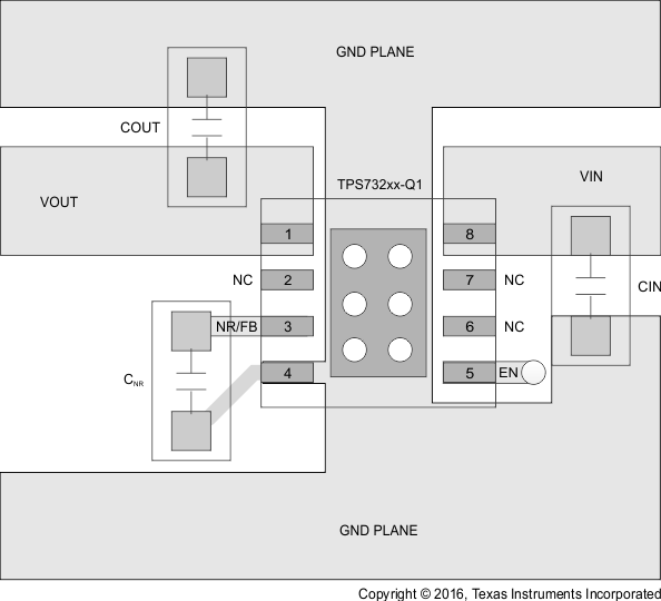
To improve ac performance such as PSRR, output noise, and transient response, TI recommends designing the PCB with separate ground planes for VIN and VOUT, with each ground plane connected only at the GND pin of the device. In addition, the ground connection for the bypass capacitor should connect directly to the GND pin of the device.
10.2 Layout Example
 Figure 34. Layout Diagram
10.3 Power Dissipation
The ability to remove heat from the die is different for each package type, presenting different considerations in the PCB layout. The PCB area around the device that is free of other components moves the heat from the device to the ambient air. Using heavier copper will increase the effectiveness in removing heat from the device. The addition of plated through-holes to heat-dissipating layers will also improve the heat-sink effectiveness.
Power dissipation depends on input voltage and load conditions. Power dissipation is equal to the product of the output current times the voltage drop across the output pass element (VIN to VOUT):

Power dissipation can be minimized by using the lowest possible input voltage necessary to assure the required output voltage.
10.4 Package Mounting
Solder pad footprint recommendations for the TPS732-Q1 family of devices are presented in the Solder Pad Recommendations for Surface-Mount Devices (SBFA015) application bulletin.