JAJS408M June 2008 – June 2018 TPS735
PRODUCTION DATA.
- 1 特長
- 2 アプリケーション
- 3 概要
- 4 改訂履歴
- 5 Specifications
- 6 Detailed Description
- 7 Application and Implementation
- 8 Power Supply Recommendations
- 9 Layout
- 10デバイスおよびドキュメントのサポート
- 11メカニカル、パッケージ、および注文情報
パッケージ・オプション
メカニカル・データ(パッケージ|ピン)
サーマルパッド・メカニカル・データ
発注情報
9.3 Power Dissipation
The ability to remove heat from the die is different for each package type, which presents different considerations in the PCB layout. The PCB area around the device that is free of other components moves the heat from the device to the ambient air. Performance data for JEDEC low- and high-K boards are shown in the Thermal Information section. Heavier copper increases the effectiveness in removing heat from the device. The addition of plated through-holes to heat-dissipating layers improves the heat sink effectiveness.
Power dissipation depends on input voltage and load conditions. Power dissipation can be approximated by the product of the output current and the voltage drop across the output pass element, as Equation 2 shows.
NOTE
When the device is used in a condition of high input and low output voltages, PD can exceed the junction temperature rating even when the ambient temperature is at room temperature.
Equation 3 is an example calculation for the power dissipation (PD) of the DRB package.
Power dissipation can be minimized and greater efficiency can be achieved by using the lowest possible input voltage necessary to achieve the required output performance.
On the DRB package, the primary conduction path for heat is through the exposed thermal pad to the PCB. The pad can be connected to ground or left floating. The pad must be attached to an appropriate amount of copper PCB area to ensure that the device does not overheat. The maximum allowable junction-to-ambient thermal resistance depends on the maximum ambient temperature, maximum device junction temperature, and power dissipation of the device. Equation 4 calculates the maximum junction-to-ambient thermal resistance.

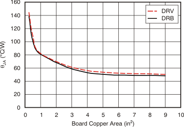
Figure 23 estimates the maximum RθJA and the minimum amount of PCB copper area required to heat sink.

NOTE:
θJA value at board size of 9 in2 (that is, 3 in × 3 in) is a JEDEC standard.Figure 23 shows the variation of θJA as a function of ground plane copper area in the board. It is intended only as a guideline to demonstrate the effects of heat spreading in the ground plane and must not be used to estimate actual thermal performance in real application environments.
NOTE
When the device is mounted on an application PCB, it is strongly recommended to use ΨJT and ΨJB, as explained in the Estimating Junction Temperature section.

