JAJS408M June 2008 – June 2018 TPS735
PRODUCTION DATA.
- 1 特長
- 2 アプリケーション
- 3 概要
- 4 改訂履歴
- 5 Specifications
- 6 Detailed Description
- 7 Application and Implementation
- 8 Power Supply Recommendations
- 9 Layout
- 10デバイスおよびドキュメントのサポート
- 11メカニカル、パッケージ、および注文情報
パッケージ・オプション
メカニカル・データ(パッケージ|ピン)
サーマルパッド・メカニカル・データ
発注情報
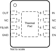
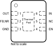
Pin Configuration and Functions
Pin Functions
| PIN | I/O | DESCRIPTION | ||
|---|---|---|---|---|
| NAME | NO | |||
| DRV | DRB | |||
| IN | 6 | 8 | I | Input supply. A 0.1-µF to 1-µF, low ESR capacitor must be placed from this pin to ground near the device. |
| GND | 3 | 4 | — | Ground. The pad must be tied to GND. |
| EN | 4 | 5 | I | Driving the enable pin (EN) high turns on the regulator. Driving this pin low puts the regulator into shutdown mode. The EN pin can be connected to the IN pin if not used. |
| NR | 2 | 3 | — | This pin is only available for the fixed voltage versions. Connecting an external capacitor to this pin bypasses noise that is generated by the internal band gap and allows the output noise to be reduced to very low levels. The maximum recommended capacitor is 0.01 μF. |
| FB | 2 | 3 | I | This pin is only available for the adjustable version. The FB pin is the input to the control-loop error amplifier, and is used to set the output voltage of the device. This pin must not be left floating. |
| OUT | 1 | 1 | O | This pin is the output of the regulator. A small, 2.2-μF ceramic capacitor is required from this pin to ground to assure stability. The minimum output capacitance required for stability is 2 µF. |
| NC | 5 | 2, 6, 7 | — | Not internally connected. |
| Thermal pad | — | |||

