SGLS247B September 2011 – March 2016 TPS763-Q1
PRODUCTION DATA.
- 1 Features
- 2 Applications
- 3 Description
- 4 Revision History
- 5 Voltage Options
- 6 Pin Configuration and Functions
- 7 Specifications
- 8 Detailed Description
- 9 Application and Implementation
- 10Power Supply Recommendations
- 11Layout
- 12Device and Documentation Support
- 13Mechanical, Packaging, and Orderable Information
パッケージ・オプション
デバイスごとのパッケージ図は、PDF版データシートをご参照ください。
メカニカル・データ(パッケージ|ピン)
- DBV|5
サーマルパッド・メカニカル・データ
発注情報
8 Detailed Description
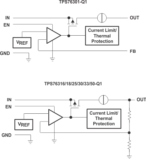
8.1 Overview
The TPS763xx-Q1 low-dropout (LDO) regulators are new families of regulators which have been optimized for use in battery-operated equipment and feature low dropout voltages, low quiescent current (140 μA), and an enable input to reduce supply currents to less than 2 μA when the regulator is turned off.
8.2 Functional Block Diagram

8.3 Feature Description
8.3.1 Regulator Protection
The TPS763xx-Q1 pass element has a built-in back diode that safely conducts reverse currents when the input voltage drops below the output voltage (for example, during power down). Current is conducted from the output to the input and is not internally limited. If extended reverse voltage is anticipated, external limiting might be appropriate.
The TPS763xx-Q1 also features internal current limiting and thermal protection. During normal operation, the TPS763xx-Q1 limits output current to approximately 800 mA. When current limiting engages, the output voltage scales back linearly until the overcurrent condition ends. While current limiting is designed to prevent gross device failure, care should be taken not to exceed the power dissipation ratings of the package. If the temperature of the device exceeds 165°C, thermal-protection circuitry shuts it down. Once the device has cooled down to below 140°C, the regulator operation resumes.
8.4 Device Functional Modes
8.4.1 Normal Operation
The device regulates to the nominal output voltage under the following conditions:
- The input voltage is at least as high as VIN(min).
- The input voltage is greater than the nominal output voltage added to the dropout voltage.
- The enable voltage is greater than VEN(min).
- The output current is less than the current limit.
- The device junction temperature is less than the maximum specified junction temperature.
8.4.2 Dropout Operation
If the input voltage is lower than the nominal output voltage plus the specified dropout voltage, but all other conditions are met for normal operation, the device operates in dropout mode. In this mode of operation, the output voltage is the same as the input voltage minus the dropout voltage. The transient performance of the device is significantly degraded because the pass device is in the linear region and no longer controls the current through the LDO. Line or load transients in dropout can result in large output voltage deviations.
8.4.3 Disabled
The device is disabled under the following conditions:
- The enable voltage is less than the enable falling threshold voltage or has not yet exceeded the enable rising threshold.
- The device junction temperature is greater than the thermal shutdown temperature.
- The input voltage is less than UVLOfalling.
Table 1 shows the conditions that lead to the different modes of operation.
Table 1. Device Functional Mode Comparison
| OPERATING MODE | PARAMETER | |||
|---|---|---|---|---|
| VIN | VEN | IOUT | TJ | |
| Normal mode | VIN > VOUT(nom) + VDO and VIN > VIN(min) | VEN > VEN(high) | IOUT < ILIM | TJ < 125°C |
| Dropout mode | VIN(min) < VIN < VOUT(nom) + VDO | VEN > VEN(high) | — | TJ < 125°C |
| Disabled mode (any true condition disables the device) | VIN < UVLOfalling | VEN < VEN(low) | — | TJ > 165°C(1) |