SLVS332J March 2001 – December 2016
PRODUCTION DATA.
8 Application and Implementation
NOTE
Information in the following applications sections is not part of the TI component specification, and TI does not warrant its accuracy or completeness. TI’s customers are responsible for determining suitability of components for their purposes. Customers should validate and test their design implementation to confirm system functionality.
8.1 Application Information
The TPS797xx family of low-dropout (LDO) regulators are optimized for micropower applications. The family features extremely low dropout voltages and ultra-low quiescent current (typically 1.2-µA ).
8.2 Typical Application
8.2.1 Powering Microcontrollers
This device is suited to provide a regulated input voltage and power good (PG) supervisory signal to low-power devices such as mixed-signal microcontrollers. The quiescent (or ground) current of the TPS797xx family is typically 1.2 µA, even at full load; therefore, the reduction in battery life by including the TPS797xx in the system is negligible.
Figure 11 shows an application where the TPS79718 powers TI’s MSP430 mixed signal microcontroller.
Minimal board space is required to accommodate the DCK (SC70) packaged TPS79718, the 0.1-µF output capacitor, the 0.47-µF input capacitor, and the pullup resistor on the PG pin.
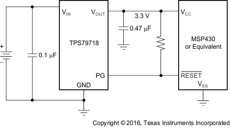 Figure 11. MSP430 Microcontroller Powered by the TPS79718 Regulator Diagram
8.2.1.1 Design Requirements
Table 2 lists the design parameters for this example.
Table 2. Design Parameters
| PARAMETER | VALUE |
|---|---|
| Input voltage range | 3.5 V to 5.5 V |
| Output voltage | 3.3 V |
| Output current rating | 50 mA |
| Minimum output capacitor | 0.47 µF |
8.2.1.2 Detailed Design Procedure
8.2.1.2.1 External Capacitor Requirements
Although not required, an input bypass capacitor with a value of 0.1-µF or larger (connected between IN and GND and placed close to the TPS797xx) is recommended, especially when a highly resistive power supply is powering the LDO in addition to other devices. Like all low-dropout regulators, the TPS797xx requires an output capacitor connected between OUT and GND to stabilize the internal control loop. The minimum recommended capacitance is 0.47-µF. Any 0.47-µF capacitor is suitable, and capacitor values larger than 0.47-µF are acceptable.
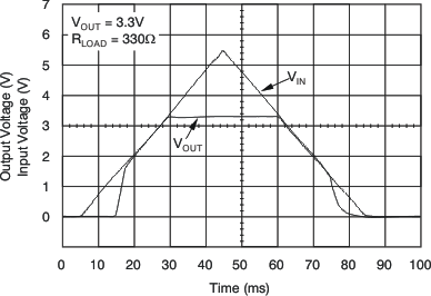
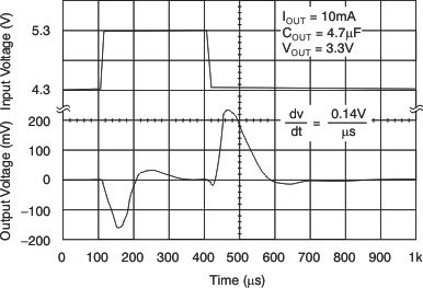
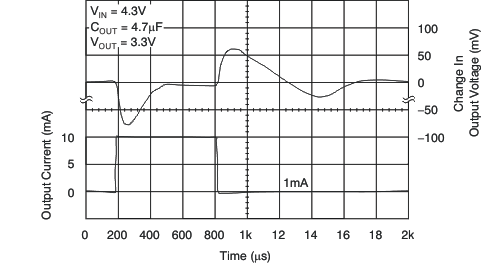
8.2.1.3 Application Curves
over operating temperature range TJ = –40°C to 85°C, typical values are at TA = 25°C, VI = VO (typical) + 0.5 V or 2 V (whichever is greater); IO = 0.5 mA, VEN = VI, and CO = 1 µF (unless otherwise noted)
