SLVS332J March   2001  – December 2016

PRODUCTION DATA.  

  1. Features
  2. Applications
  3. Description
  4. Revision History
  5. Pin Configuration and Functions
  6. Specifications
    1. 6.1 Absolute Maximum Ratings
    2. 6.2 ESD Ratings
    3. 6.3 Recommended Operating Conditions
    4. 6.4 Thermal Information
    5. 6.5 Electrical Characteristics
    6. 6.6 Typical Characteristics
  7. Detailed Description
    1. 7.1 Overview
    2. 7.2 Functional Block Diagram
    3. 7.3 Feature Description
      1. 7.3.1 Regulator Protection
    4. 7.4 Device Functional Modes
  8. Application and Implementation
    1. 8.1 Application Information
    2. 8.2 Typical Application
      1. 8.2.1 Powering Microcontrollers
        1. 8.2.1.1 Design Requirements
        2. 8.2.1.2 Detailed Design Procedure
          1. 8.2.1.2.1 External Capacitor Requirements
        3. 8.2.1.3 Application Curves
  9. Power-Supply Recommendations
  10. 10Layout
    1. 10.1 Layout Guidelines
    2. 10.2 Layout Example
    3. 10.3 Power Dissipation and Junction Temperature
  11. 11Device and Documentation Support
    1. 11.1 Related Links
    2. 11.2 Receiving Notification of Documentation Updates
    3. 11.3 Community Resources
    4. 11.4 Trademarks
    5. 11.5 Electrostatic Discharge Caution
    6. 11.6 Glossary
  12. 12Mechanical, Packaging, and Orderable Information

パッケージ・オプション

メカニカル・データ(パッケージ|ピン)
サーマルパッド・メカニカル・データ
発注情報

Detailed Description

Overview

The TPS797xx devices offer a low-dropout voltage, ultra-low-power operation, and are stable with any capacitor greater than 0.47 µF, and contains an integrated open-drain power good (PG) output.

Functional Block Diagram

TPS79718 TPS797285 TPS79730 TPS79733 func_blk_lvs332.gif

Feature Description

Regulator Protection

The TPS797xx PMOS-pass transistor has a built-in back diode that conducts reverse current when the input voltage drops below the output voltage (for example, during power down). Current is conducted from the output to the input and is not internally limited. If extended reverse voltage operation is anticipated, external limiting might be appropriate.

The TPS797xx features internal current limiting. During normal operation, the TPS797xx limits output current to approximately 190 mA. When current limiting engages, the output voltage scales back linearly until the overcurrent condition ends. Take care not to exceed the power dissipation ratings of the package.

Device Functional Modes

Table 1 provides a quick comparison between the normal, dropout, and disabled modes of operation.
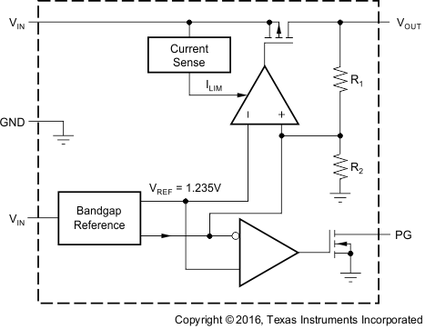
Table 1. Device Modes Comparison

OPERATING MODE PARAMETER
VI IOUTx
Normal(1) VI > VO + V(DO) IOUTx < ISC
Dropout(1) VI < VO + V(DO) IOUTx < ISC
All table conditions must be met.