SLVS332J March 2001 – December 2016
PRODUCTION DATA.
10 Layout
10.1 Layout Guidelines
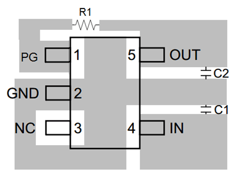
General guidelines for linear regulator designs are to place all circuit components on the same side of the circuit board and as near as practical to the respective LDO pin connections. Place ground return connections to the input and output capacitor, and to the LDO ground pin as close to each other as possible, connected by a wide, component-side, copper surface. The use of vias and long traces to create LDO circuit connections is strongly discouraged and negatively affects system performance.
10.2 Layout Example
 Figure 16. Layout Example
10.3 Power Dissipation and Junction Temperature
Specified regulator operation is ensured for a junction temperature of up to 85°C; restrict the maximum junction temperature to 85°C under normal operating conditions. This restriction limits the power dissipation the regulator can handle in any given application. To ensure the junction temperature is within acceptable limits, calculate the maximum allowable dissipation (PD(MAX)) and the actual dissipation (PD), which must be less than or equal to PD(MAX).
The maximum-power-dissipation limit is determined using Equation 1.

where
- TJ(max) is the maximum allowable junction temperature
- RθJA is the thermal resistance junction-to-ambient for the package (see Thermal Information)
- TA is the ambient temperature
The regulator dissipation is calculated using Equation 2.

Power dissipation resulting from quiescent current is negligible.