SLVS332J March   2001  – December 2016

PRODUCTION DATA.  

  1. Features
  2. Applications
  3. Description
  4. Revision History
  5. Pin Configuration and Functions
  6. Specifications
    1. 6.1 Absolute Maximum Ratings
    2. 6.2 ESD Ratings
    3. 6.3 Recommended Operating Conditions
    4. 6.4 Thermal Information
    5. 6.5 Electrical Characteristics
    6. 6.6 Typical Characteristics
  7. Detailed Description
    1. 7.1 Overview
    2. 7.2 Functional Block Diagram
    3. 7.3 Feature Description
      1. 7.3.1 Regulator Protection
    4. 7.4 Device Functional Modes
  8. Application and Implementation
    1. 8.1 Application Information
    2. 8.2 Typical Application
      1. 8.2.1 Powering Microcontrollers
        1. 8.2.1.1 Design Requirements
        2. 8.2.1.2 Detailed Design Procedure
          1. 8.2.1.2.1 External Capacitor Requirements
        3. 8.2.1.3 Application Curves
  9. Power-Supply Recommendations
  10. 10Layout
    1. 10.1 Layout Guidelines
    2. 10.2 Layout Example
    3. 10.3 Power Dissipation and Junction Temperature
  11. 11Device and Documentation Support
    1. 11.1 Related Links
    2. 11.2 Receiving Notification of Documentation Updates
    3. 11.3 Community Resources
    4. 11.4 Trademarks
    5. 11.5 Electrostatic Discharge Caution
    6. 11.6 Glossary
  12. 12Mechanical, Packaging, and Orderable Information

パッケージ・オプション

メカニカル・データ(パッケージ|ピン)
サーマルパッド・メカニカル・データ
発注情報

Pin Configuration and Functions

DCK Package
5-Pin SC70
Top View
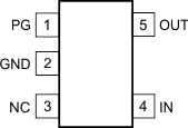
TPS79718 TPS797285 TPS79730 TPS79733 po_slvs332.gif

Pin Functions

PIN I/O DESCRIPTION
NO. NAME
1 PG O The PG pin for the fixed voltage option devices is an open drain, active-high output that indicates the status of VO (output of the LDO). When VO exceeds approximately 90% of the regulated voltage, PG goes to a high-impedance state. PG goes to a low-impedance state when VO falls below approximately 90% (that is, overload condition) of the regulated voltage. The open drain output of the PG pin requires a pullup resistor.
2 GND Ground
3 NC No connection
4 IN I The IN pin is the power-supply input to the device.
5 OUT O The OUT pin provides the regulated output voltage of the device.