JAJSET0B December   2018  – October 2019 TPS7A26

PRODUCTION DATA.  

  1. 特長
  2. アプリケーション
  3. 概要
    1.     Device Images
      1.      代表的なアプリケーション回路
  4. 改訂履歴
  5. 概要(続き)
  6. Pin Configuration and Functions
    1.     Pin Functions
  7. Specifications
    1. 7.1 Absolute Maximum Ratings
    2. 7.2 ESD Ratings
    3. 7.3 Recommended Operating Conditions
    4. 7.4 Thermal Information
    5. 7.5 Electrical Characteristics
    6. 7.6 Typical Characteristics
  8. Detailed Description
    1. 8.1 Overview
    2. 8.2 Functional Block Diagram
    3. 8.3 Feature Description
      1. 8.3.1 Output Enable
      2. 8.3.2 Dropout Voltage
      3. 8.3.3 Current Limit
      4. 8.3.4 Undervoltage Lockout (UVLO)
      5. 8.3.5 Thermal Shutdown
      6. 8.3.6 Power Good
      7. 8.3.7 Active Overshoot Pulldown Circuitry
    4. 8.4 Device Functional Modes
      1. 8.4.1 Device Functional Mode Comparison
      2. 8.4.2 Normal Operation
      3. 8.4.3 Dropout Operation
      4. 8.4.4 Disabled
  9. Application and Implementation
    1. 9.1 Application Information
      1. 9.1.1 Adjustable Device Feedback Resistors
      2. 9.1.2 Recommended Capacitor Types
      3. 9.1.3 Input and Output Capacitor Requirements
      4. 9.1.4 Reverse Current
      5. 9.1.5 Feed-Forward Capacitor (CFF)
      6. 9.1.6 Power Dissipation (PD)
      7. 9.1.7 Estimating Junction Temperature
      8. 9.1.8 Special Consideration for Line Transient
    2. 9.2 Typical Application
      1. 9.2.1 Design Requirements
      2. 9.2.2 Detailed Design Procedure
        1. 9.2.2.1 Transient Response
        2. 9.2.2.2 Selecting Feedback Divider Resistors
        3. 9.2.2.3 Thermal Dissipation
      3. 9.2.3 Application Curve
  10. 10Power Supply Recommendations
  11. 11Layout
    1. 11.1 Layout Guidelines
    2. 11.2 Layout Examples
  12. 12デバイスおよびドキュメントのサポート
    1. 12.1 デバイス・サポート
      1. 12.1.1 デバイスの項目表記
    2. 12.2 ドキュメントのサポート
      1. 12.2.1 関連資料
    3. 12.3 ドキュメントの更新通知を受け取る方法
    4. 12.4 コミュニティ・リソース
    5. 12.5 商標
    6. 12.6 静電気放電に関する注意事項
    7. 12.7 Glossary
  13. 13メカニカル、パッケージ、および注文情報

パッケージ・オプション

デバイスごとのパッケージ図は、PDF版データシートをご参照ください。

メカニカル・データ(パッケージ|ピン)
  • DRV|6
サーマルパッド・メカニカル・データ
発注情報

Current Limit

The device has an internal current limit circuit that protects the regulator during transient high-load current faults or shorting events. The current limit is a brickwall scheme. In a high-load current fault, the brickwall scheme limits the output current to the current limit (ICL). ICL is listed in the Electrical Characteristics table.

The output voltage is not regulated when the device is in current limit. When a current limit event occurs, the device begins to heat up because of the increase in power dissipation. When the device is in brickwall current limit, the pass transistor dissipates power [(VIN – VOUT) × ICL]. If thermal shutdown is triggered, the device turns off. After the device cools down, the internal thermal shutdown circuit turns the device back on. If the output current fault condition continues, the device cycles between current limit and thermal shutdown. For more information on current limits, see the Know Your Limits application report.

Figure 36 shows a diagram of the current limit.
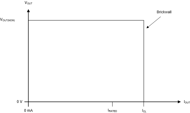
TPS7A26 tps7a26-current-limit.gifFigure 36. Current Limit