SBVS204F June 2012 – September 2014
PRODUCTION DATA.
- 1 Features
- 2 Applications
- 3 Description
- 4 Revision History
- 5 Pin Configuration and Functions
- 6 Specifications
- 7 Detailed Description
- 8 Application and Implementation
- 9 Power Supply Recommendations
- 10Layout
- 11Device and Documentation Support
- 12Mechanical, Packaging, and Orderable Information
1 Features
- Input Voltage Range: +3 V to +36 V
- Output Voltage Noise:
4 µVRMS (10 Hz, 100 kHz) - Power-Supply Ripple Rejection:
- 82 dB (100 Hz)
- ≥ 55 dB (10 Hz, 10 MHz)
- Two Output Voltage Modes:
- ANY-OUT™ Version (User-Programmable Output via PCB Layout):
- No External Feedback Resistors or Feed-Forward Capacitors Required
- Output Voltage Range: +1.4 V to +20.5 V
- Adjustable Version (TPS7A4701 only):
- Output Voltage Range: +1.4 V to +34 V
- ANY-OUT™ Version (User-Programmable Output via PCB Layout):
- Output Current: 1 A
- Dropout Voltage: 307 mV at 1 A
- CMOS Logic Level-Compatible Enable Pin
- Built-In Fixed Current Limit and
Thermal Shutdown - Available in High-Performance Thermal Package: 5-mm × 5-mm QFN
- Operating Temperature Range:
–40°C to 125°C
2 Applications
- Voltage-Controlled Oscillators (VCO)
- Frequency Synthesizers
- Test and Measurement
- Instrumentation, Medical, and Audio
- RX, TX, and PA Circuitry
- Supply Rails for Operational Amplifiers,
DACs, ADCs, and Other High-Precision Analog Circuitry - Post DC-DC Converter Regulation and
Ripple Filtering - Base Stations and Telecom Infrastructure
- +12-V and +24-V Industrial Buses
3 Description
The TPS7A47 is a family of positive voltage (+36 V), ultralow-noise (4 µVRMS) low-dropout linear regulators (LDO) capable of sourcing a 1-A load.
The TPS7A4700 output voltages are user-programmable (up to 20.5 V) using a printed circuit board (PCB) layout without the need of external resistors or feed-forward capacitors, thus reducing overall component count.
The TPS7A4701 output voltage can be configured with a user-programmable PCB layout (up to 20.5 V), or adjustable (up to 34 V) with external feedback resistors.
The TPS7A47 is designed with bipolar technology primarily for high-accuracy, high-precision instrumentation applications where clean voltage rails are critical to maximize system performance. This feature makes the device ideal for powering operational amplifiers, analog-to-digital converters (ADCs), digital-to-analog converters (DACs), and other high-performance analog circuitry in critical applications such as medical, radio frequency (RF), and test-and-measurement.
In addition, the TPS7A47 is ideal for post dc-dc converter regulation. By filtering out the output voltage ripple inherent to dc-dc switching conversions, maximum system performance is ensured in sensitive instrumentation, test-and-measurement, audio, and RF applications.
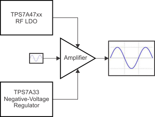
For applications where positive and negative low-noise rails are required, consider TI's TPS7A33 family of negative high-voltage, ultralow-noise linear regulators.
Device Information(1)
| PART NUMBER | PACKAGE | BODY SIZE (NOM) |
|---|---|---|
| TPS7A470x | VQFN (20) | 5 mm × 5 mm |
- For all available packages, see the orderable addendum at the end of the datasheet.
4 Revision History
Changes from E Revision (January 2014) to F Revision
- Added Handling Rating table, Feature Description section, Device Functional Modes, Application and Implementation section, Power Supply Recommendations section, Layout section, Device and Documentation Support section, and Mechanical, Packaging, and Orderable Information section Go
- Reworded ninth bullet in Features listGo
- Changed polarity of op amp shown on right side of the functional block diagram Go
- Reworded second paragraph in Soft-Start And Inrush Current section Go
- Revised Capacitor Recommendations sectionGo
- Changed paragraph 2 of Dropout Voltage (VDO) section for clarity Go
- Revised paragraph 1 of Startup section Go
- Rewrote paragraph 1 of Power-Supply Rejection Ratio (PSRR) section to eliminate confusion Go
- Changed paragraph 1 of Power Supply Recommendations section Go
- Changed paragraph 1 and paragraph 4 of Power Dissipation (PD) sectionGo
- Revised paragraph 2 of Layout Guidelines section Go
- Changed second paragraph of Thermal Protection section Go
Changes from D Revision (December 2013) to E Revision
- Changed Output Voltage Noise value from 4.17 µV to 4 µV in three instances on front pageGo
- Changed 2nd and 3rd paragraphs of Description sectionGo
- Added "Thermal Pad" to pin configuration drawingGo
- Changed EN pin descriptionGo
- Changed SENSE/FB pin to be for TPS7A4701 onlyGo
- Added new row to Pin Descriptions table for SENSE pin (for TPS7A4700 only)Go
- Added new row to Pin Descriptions table for thermal padGo
- Added VREF parameterGo
- Added TPS7A4701 device to test conditions for VNR parameterGo
- Added Feedback Pin Current parameter to Electrical Characteristics Go
- Deleted Dropout Voltage vs Output Current graphGo
- Added EN pin to Functional Block DiagramGo
- Added sentence to ANY-OUT Programmable Output Voltage section to clarify ANY-OUT is for both devicesGo
- Changed last two paragraphs of Adjustable Operation sectionGo
- Added "TPS7A4701 Only" to Adjustable Operation section titleGo
- Deleted equation in Figure 23Go
- Changed Equation 3Go
Changes from C Revision (July 2013) to D Revision
- Changed data sheeet status from production mix to production dataGo
- Changed TPS7A4701 ESD rating from > 1 kV to 2.5 kVGo
- Changed noise reduction pin voltage parameter to show both devicesGo
- Added text clarifying VREF typical value to last paragraph on pageGo
Changes from B Revision (April 2013) to C Revision
- Deleted TPS7A4702 preview device from data sheetGo
Changes from A Revision (July 2012) to B Revision
- Changed TPS7A47 to TPS7A4700Go
- Added TPS7A4701 and TPS7A4702 preview devices to data sheetGo
- Changed front-page figureGo
- Added FB to SENSE pin to Functional Block DiagramGo
- Added new paragraph after Table 1Go
- Added new Table 2Go
- Added Adjustable Operation sectionGo
Changes from * Revision (June 2012) to A Revision
- Moved to full production data (changes throughout document)Go