SBVS204F June 2012 – September 2014
PRODUCTION DATA.
- 1 Features
- 2 Applications
- 3 Description
- 4 Revision History
- 5 Pin Configuration and Functions
- 6 Specifications
- 7 Detailed Description
- 8 Application and Implementation
- 9 Power Supply Recommendations
- 10Layout
- 11Device and Documentation Support
- 12Mechanical, Packaging, and Orderable Information
7 Detailed Description
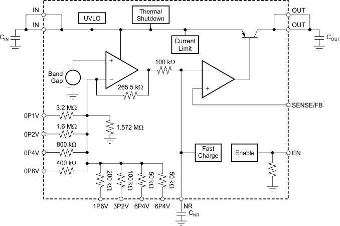
7.1 Overview
The TPS7A4700 and TPS7A4701 (TPS7A470x) are positive voltage (+36 V), ultralow-noise (4 µVRMS) LDOs capable of sourcing a 1-A load. The TPS7A470x is designed with bipolar technology primarily for high-accuracy, high-precision instrumentation applications where clean voltage rails are critical to maximize system performance. This feature makes the device ideal for powering operational amplifiers, analog-to-digital converters (ADCs), digital-to-analog converters (DACs), and other high-performance analog circuitry.
7.3 Feature Description
7.3.1 Internal Current Limit (ICL)
The internal current limit circuit is used to protect the LDO against high-load current faults or shorting events. The LDO is not designed to operate at a steady-state current limit. During a current-limit event, the LDO sources constant current. Therefore, the output voltage falls while load impedance decreases. Note also that when a current limit occurs while the resulting output voltage is low, excessive power is dissipated across the LDO, which results in a thermal shutdown of the output.
7.3.2 Enable (EN) And Under-Voltage Lockout (UVLO)
The TPS7A470x only turns on when both EN and UVLO are above the respective voltage thresholds. The UVLO circuit monitors input voltage (VI) to prevent device turn-on before VI rises above the lockout voltage. The UVLO circuit also causes a shutdown when VI falls below lockout. The EN signal allows independent logic-level turn-on and shutdown of the LDO when the input voltage is present. EN can be connected directly to VI if independent turn-on is not needed.
7.3.3 Soft-Start And Inrush Current
Soft-start refers to the ramp-up characteristic of the output voltage during LDO turn-on after EN and UVLO have achieved threshold voltage. The noise reduction capacitor serves a dual purpose of both governing output noise reduction and programming the soft-start ramp during turn-on.
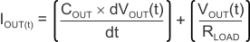
Inrush current is defined as the current through the LDO from IN to OUT during the time of the turn-on ramp up. Inrush current then consists primarily of the sum of load and charge current to the output capacitor. Inrush current can be estimated by Equation 1:
where
7.4 Device Functional Modes
The TPS7A470x has the following functional modes:
- Enabled: When EN goes above V+EN(HI), the device is enabled.
- Disabled: When EN goes below V+EN(LO), the device is disabled. During this time, OUT is high impedance, and the current into IN does not exceed I(SHDN).
7.5 Programming
7.5.1 ANY-OUT Programmable Output Voltage
Both devices can be used in ANY-OUT mode. For ANY-OUT operation, the TPS7A4700 and TPS7A4701 do not use external resistors to set the output voltage, but use device pins 4, 5, 6, 8, 9, 10, 11, and 12 to program the regulated output voltage. Each pin is either connected to ground (active) or is left open (floating). The ANY-OUT programming is set by Equation 2 as the sum of the internal reference voltage (V(REF) = 1.4 V) plus the accumulated sum of the respective voltages assigned to each active pin; that is, 100 mV (pin 12), 200 mV (pin 11), 400 mV (pin 10), 800 mV (pin 9), 1.6 V (pin 8), 3.2 V (pin 6), 6.4 V (pin 5), or 6.4 V (pin 4). Table 1 summarizes these voltage values associated with each active pin setting for reference. By leaving all program pins open, or floating, the output is thereby programmed to the minimum possible output voltage equal to V(REF).

Table 1. ANY-OUT Programmable Output Voltage
| ANY-OUT PROGRAM PINS (Active Low) | ADDITIVE OUTPUT VOLTAGE LEVEL |
|---|---|
| Pin 4 (6P4V2) | 6.4 V |
| Pin 5 (6P4V1) | 6.4 V |
| Pin 6 (3P2) | 3.2 V |
| Pin 8 (1P6) | 1.6 V |
| Pin 9 (0P8) | 800 mV |
| Pin 10 (0P4) | 400 mV |
| Pin 11 (0P2) | 200 mV |
| Pin 12 (0P1) | 100 mV |
Table 2 shows a list of the most common output voltages and the corresponding pin settings. The voltage setting pins have a binary weight; therefore, the output voltage can be programmed to any value from 1.4 V to 20.5 V in 100-mV steps.
Table 2. Common Output Voltages and Corresponding Pin Settings
| VO (V) | PIN NAMES AND VOLTAGE PER PIN | |||||||
|---|---|---|---|---|---|---|---|---|
| 0P1V 100 mV |
0P2V 200 mV |
0P4V 400 mV |
0P8V 800 mV |
1P6V 1.6 V |
3P2V 3.2 V |
6P4V1 6.4 V |
6P4V2 6.4 V |
|
| 1.4 | Open | Open | Open | Open | Open | Open | Open | Open |
| 1.5 | GND | Open | Open | Open | Open | Open | Open | Open |
| 1.8 | Open | Open | GND | Open | Open | Open | Open | Open |
| 2.5 | GND | GND | Open | GND | Open | Open | Open | Open |
| 3 | Open | Open | Open | Open | GND | Open | Open | Open |
| 3.3 | GND | GND | Open | Open | GND | Open | Open | Open |
| 4.5 | GND | GND | GND | GND | GND | Open | Open | Open |
| 5 | Open | Open | GND | Open | Open | GND | Open | Open |
| 10 | Open | GND | GND | Open | GND | Open | GND | Open |
| 12 | Open | GND | Open | GND | Open | GND | GND | Open |
| 15 | Open | Open | Open | GND | Open | Open | GND | GND |
| 18 | Open | GND | GND | Open | Open | GND | GND | GND |
| 20.5 | GND | GND | GND | GND | GND | GND | GND | GND |
7.5.2 Adjustable Operation (TPS7A4701 Only)
The TPS7A4701 has an output voltage range of 1.4 V to 34 V. For adjustable operation, set the nominal output voltage of the device using two external resistors, as shown in Figure 23.
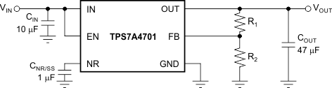
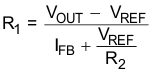
R1 and R2 can be calculated for any output voltage within the operational range. The current through feedback resistor R2 must be at least 5 µA to ensure stability. Additionally, the current into the FB pin (I(FB), typically 350 nA) creates an additional output voltage offset that depends on the resistance of R1. For high-accuracy applications, select R2 such that the current through R2 is at least 35 µA to minimize any effects of I(FB) variation on the output voltage; 10 kΩ is recommended. R1 can be calculated using Equation 3.
Use 0.1% tolerance resistors to minimize the effects of resistor inaccuracy on the output voltage.
Table 3 shows the resistor combinations to achieve some standard rail voltages with commercially-available 1% tolerance resistors. The resulting output voltages yield a nominal error of < 0.5%.
Table 3. Suggested Resistors for Common Voltage Rails
| VOUT | R1, Calculated | R1, Closest 1% Value | R2 |
|---|---|---|---|
| 1.4 V | 0 Ω | 0 Ω | ∞ |
| 1.8 V | 2.782 kΩ | 2.8 kΩ | 9.76 kΩ |
| 3.3 V | 13.213 kΩ | 13.3 kΩ | 9.76 kΩ |
| 5 V | 25.650 kΩ | 25.5 kΩ | 10 kΩ |
| 12 V | 77.032 kΩ | 76.8 kΩ | 10.2 kΩ |
| 15 V | 101.733 kΩ | 102 kΩ | 10.5 kΩ |
| 18 V | 118.276 kΩ | 118 kΩ | 10 kΩ |
| 24 V | 164.238 kΩ | 165 kΩ | 10.2 kΩ |
To achieve higher nominal accuracy, two resistors can be used in the place of R1. Select the two resistor values such that the sum results in a value as close as possible to the calculated R1 value.
There are several alternative ways to set the output voltage. The program pins can be pulled low using external general-purpose input/output pins (GPIOs), or can be hardwired by the given layout of the printed circuit board (PCB) to set the ANY-OUT voltage. The TPS7A4701 evaluation module (EVM), available for purchase from the TI eStore, allows the output voltage to be programmed using jumpers.