JAJSGA5D October 2014 – June 2019 TPS82084 , TPS82085
PRODUCTION DATA.
- 1 特長
- 2 アプリケーション
- 3 概要
- 4 改訂履歴
- 5 概要(続き)
- 6 Pin Configuration and Functions
- 7 Specifications
- 8 Detailed Description
- 9 Application and Implementation
- 10Power Supply Recommendations
- 11Layout
- 12デバイスおよびドキュメントのサポート
- 13メカニカル、パッケージ、および注文情報
パッケージ・オプション
デバイスごとのパッケージ図は、PDF版データシートをご参照ください。
メカニカル・データ(パッケージ|ピン)
- SIL|8
サーマルパッド・メカニカル・データ
発注情報
8.3.1 Power Save Mode (PSM)
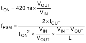
The device includes a fixed on-time (tON) circuitry. This tON, in steady-state operation in PWM and PSM modes, is estimated as:

To maintain high efficiency at light loads, the device enters Power Save Mode seamlessly when the load current decreases. This happens when the load current becomes smaller than half the inductor's ripple current. In PSM, the converter operates with a reduced switching frequency and with a minimum quiescent current to maintain high efficiency. The on time in PSM is also based on the same tON circuitry. The switching frequency in PSM is shown in Equation 1.
In PSM, the output voltage rises slightly above the nominal output voltage in PWM mode. This effect is reduced by increasing the output capacitance. The output voltage accuracy in PSM operation is reflected in the electrical specification table and given for a 22-µF output capacitor.
During PAUSE period in PSM (shown in Figure 4), the device does not change the PG pin state nor does it detect an UVLO event, in order to achieve a minimum quiescent current and maintain high efficiency at light loads.
 Figure 4. Power Save Mode Waveform Diagram