SLUSBZ6A April 2016 – August 2016 TPS92515 , TPS92515-Q1 , TPS92515HV , TPS92515HV-Q1
PRODUCTION DATA.
- 1 Features
- 2 Applications
- 3 Description
- 4 Revision History
- 5 Device Comparison Table
- 6 Pin Configuration and Functions
- 7 Specifications
-
8 Detailed Description
- 8.1 Overview
- 8.2 Functional Block Diagram
- 8.3
Feature Description
- 8.3.1 General Operation
- 8.3.2 Current Sense Comparator
- 8.3.3 OFF Timer
- 8.3.4 OFF-Timer, Shunt FET Dimming or Shunted Output Condition
- 8.3.5 Internal N-channel MOSFET
- 8.3.6 VCC Internal Regulator and Undervoltage Lockout (UVLO)
- 8.3.7 Analog Adjust Input
- 8.3.8 Thermal Protection
- 8.3.9 Junction Temperature Relative Estimation
- 8.3.10 BOOT and BOOT UVLO
- 8.3.11 PWM (UVLO and Enable)
- 8.4 Device Functional Modes
-
9 Application and Implementation
- 9.1 Application Information
- 9.2
Typical Application
- 9.2.1 General Design Procedure
- 9.2.2 Design Requirements
- 9.2.3
Detailed Design Procedure
- 9.2.3.1 Calculating Duty Cycle
- 9.2.3.2 Calculate OFF-Time Estimate
- 9.2.3.3 Calculate OFF-Time Resistor ROFF
- 9.2.3.4 Calculate the Inductance Value
- 9.2.3.5 Calculate the Sense Resistance
- 9.2.3.6 Calculate Input Capacitance
- 9.2.3.7 Verify Peak Current for Inductor Selection
- 9.2.3.8 Calculate Output Capacitance
- 9.2.3.9 Calculate UVLO Resistance Values
- 9.2.4 Application Curves
- 9.3 Dos and Don'ts
- 10Power Supply Recommendations
- 11Layout
- 12Device and Documentation Support
- 13Mechanical, Packaging, and Orderable Information
8.3.11.4 Analog and PWM Dimming - Normalized Results and Comparison
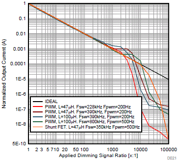
When the PWM applied signal is less than the switching cycle period and falls during an OFF-time it has no impact on the current for that cycle as the switch is already OFF. This situation can be avoided by increasing the switching frequency. Shunt FET PWM dimming avoids this issue. Current adjustment that maintains a constant ripple when shunted (see the OFF-Timer, Shunt FET Dimming or Shunted Output Condition section), creates a linear relation to the PWM shunt FET duty cycle and the average output current. Shunt FET PWM dimming can out-perform PWM dimming as characterized in Figure 27 through Figure 29, but is more complicated to implement.
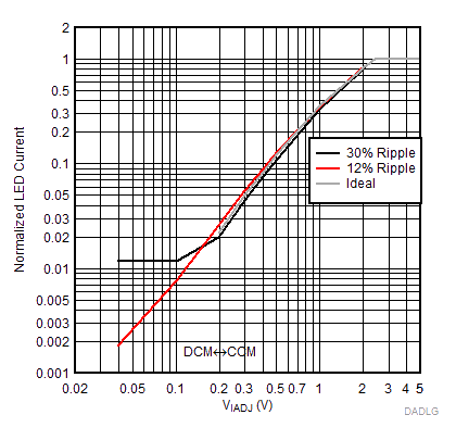
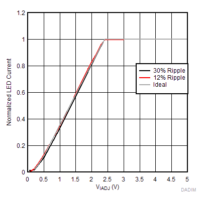
Another impact on linearity can occur when using the analog dimming function. Discontinuous conduction mode (DCM) occurs when the inductor current reaches 0 A during each cycle,. When the device enters DCM, the output current is no longer the peak current minus half the ripple. The linear range can be extended by lowering the ripple, ΔIL-PP. If the system is being digitally controlled, the applied IADJ pin voltage can be adjusted when it is known the DCM operation occurs. In either case, a lower limit is eventually reached when the measured peak threshold voltage is approximately < 50 mV. At this point, the offset error becomes a significant portion of the peak current trip point voltage being measured.


| VLED = 15 V | VIN = 55 V |

| VLED = 15 V | VIN = 55 V |