JAJSKJ1A December 2020 – February 2021 TPS929121-Q1
PRODUCTION DATA
- 1 特長
- 2 アプリケーション
- 3 概要
- 4 Revision History
- 5 Device Comparison Table
- 6 Pin Configuration and Functions
- 7 Specifications
-
8 Detailed Description
- 8.1 Overview
- 8.2 Functional Block Diagram
- 8.3
Feature Description
- 8.3.1 Device Bias and Power
- 8.3.2 Constant Current Output
- 8.3.3 PWM Dimming
- 8.3.4 On-chip 8-bit Analog-to-Digital Converter (ADC)
- 8.3.5
Diagnostic and Protection in Normal State
- 8.3.5.1 Fault Masking
- 8.3.5.2 Supply Undervoltage Lockout Diagnostics in Normal State
- 8.3.5.3 Low-Supply Warning Diagnostics in Normal State
- 8.3.5.4 Reference Diagnostics in Normal State
- 8.3.5.5 Pre-Thermal Warning and Overtemperature Protection in Normal State
- 8.3.5.6 Communication Loss Diagnostic in Normal State
- 8.3.5.7 LED Open-Circuit Diagnostics in Normal State
- 8.3.5.8 LED Short-Circuit Diagnostics in Normal State
- 8.3.5.9 On-Demand Off-State Invisible Diagnostics
- 8.3.5.10 On-Demand Off-State Single-LED Short-Circuit (SS) Diagnostics
- 8.3.5.11 Automatic Single-LED Short-Circuit (AutoSS) Detection in Normal State
- 8.3.5.12 EEPROM CRC Error in Normal State
- 48
- 8.3.6
Diagnostic and Protection in Fail-Safe States
- 8.3.6.1 Fault Masking
- 8.3.6.2 Supply UVLO Diagnostics in Fail-Safe States
- 8.3.6.3 Low-supply Warning Diagnostics in Fail-Safe states
- 8.3.6.4 Reference Diagnostics at Fail-Safe States
- 8.3.6.5 Overtemperature Protection in Fail-Safe State
- 8.3.6.6 LED Open-circuit Diagnostics in Fail-Safe State
- 8.3.6.7 LED Short-circuit Diagnostics in Fail-Safe State
- 8.3.6.8 EEPROM CRC Error in Fail-safe State
- 58
- 8.4 Device Functional Modes
- 8.5 Programming
- 8.6 Register Maps
- 9 Application and Implementation
- 10Power Supply Recommendations
- 11Layout
- 12Device and Documentation Support
- 13Mechanical, Packaging, and Orderable Information
パッケージ・オプション
メカニカル・データ(パッケージ|ピン)
- PWP|24
サーマルパッド・メカニカル・データ
- PWP|24
発注情報
8.3.5.10 On-Demand Off-State Single-LED Short-Circuit (SS) Diagnostics
To provide single-LED short-circuit diagnostics, the TPS929121-Q1 uses internal ADC to compare the output channel voltage with respect to pre-set threshold V(ADCSHORTTH).
Setting the register CONF_SSSTART to 1 starts the diagnostics immediately. The CONF_SSSTART returns to 0 in the next clock cycle. Once the diagnostics starts, the on-demand diagnostics ready flag FLAG_ODREADY are cleared to 0. Once the diagnostics finished, the FLAG_ODREADY are set to 1.
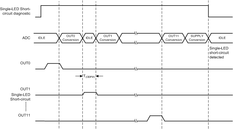
In off-state single-LED short-circuit diagnostics, once the master controller initiates single-LED short-circuit diagnostics by setting the register CONF_SSSTART, the device sequentially turns on all outputs starting from OUT0 with DC current I(ODIOUT) programed by register CONF_ODIOUT and pulse width T(ODPW) programmable by CONF_ODPW. At the end of pulse, the device initiates an AD conversion. As long as the completion of ADC conversion, the result are compared with pre-set threshold V(ADCSHORTTH) and start the diagnostics for the next channel. After all channels have been checked, the TPS929121-Q1 also checks if the supply voltage is over V(ADCLOWSUPTH) to make sure the device is not in low-dropout conditions. If the supply voltage is truly lower than V(ADCLOWSUPTH), the single-LED short-circuit fault cannot be detected and reported. If the supply voltage is high enough, and any one channel output voltage is less than pre-set threshold V(ADCSHORTTH), the TPS92910-Q1 pulls the ERR pin down with pulsed current sink for 50 µs to report fault and set the flag register including FLAG_ODDIAGCHx, FLAG_OUT and FLAG_ERR to 1. The master controller must write 1 to CLR_FAULT register to clear the fault flags after fault removal is verified by another on-demand off-state single-LED short-circuit diagnostic.
The configurable DC current I(ODIOUT) and pulse width T(ODPW) can be used to minimize the optical impact during on-demand diagnostics. TI recommends using the normal current setting and short pulse-width to avoid visible pulse; however, the parasitic capacitance impact at each output must taken care of to leave enough charging time and avoid false alarm. Low DC current setting also reduces LED forward voltage, which also affects the integrity of the detection. Thus the threshold set by CONF_ADCSHORTTH must be selected carefully. Setting CONF_ODIOUT to 0xFh uses the channel current setting by register CONF_IOUTx as on-demand pulse current.
The V(ADCSHORTTH) can be calculated with Equation 7.

where
- a = 0.2878 V.
- k = 0.1583 V/LSB.
- CONF_ADCSHORTTH is decimal number from 0 to 255.
 Figure 8-5 Single-LED Short-Circuit Off-state Timing Sequence