SCDS225B March 2007 – January 2015 TS3A44159
PRODUCTION DATA.
- 1 Features
- 2 Applications
- 3 Description
- 4 Revision History
- 5 Pin Configuration and Functions
-
6 Specifications
- 6.1 Absolute Maximum Ratings
- 6.2 ESD Ratings
- 6.3 Recommended Operating Conditions
- 6.4 Thermal Information
- 6.5 Electrical Characteristics for 1.8-V Supply
- 6.6 Electrical Characteristics for 2.1-V Supply
- 6.7 Electrical Characteristics for 2.5-V Supply
- 6.8 Electrical Characteristics for 3.3-V Supply
- 6.9 Electrical Characteristics for 4.3-V Supply
- 6.10 Typical Characteristics
- 7 Parameter Measurement Information
- 8 Detailed Description
- 9 Application and Implementation
- 10Power Supply Recommendations
- 11Layout
- 12Device and Documentation Support
- 13Mechanical, Packaging, and Orderable Information
パッケージ・オプション
デバイスごとのパッケージ図は、PDF版データシートをご参照ください。
メカニカル・データ(パッケージ|ピン)
- PW|16
- RGT|16
- RSV|16
サーマルパッド・メカニカル・データ
- RGT|16
発注情報
11 Layout
11.1 Layout Guidelines
High-speed switches require proper layout and design procedures for optimum performance. Reduce stray inductance and capacitance by keeping traces short and wide. Ensure that bypass capacitors are as close to the device as possible. Use large ground planes where possible.
11.2 Layout Example
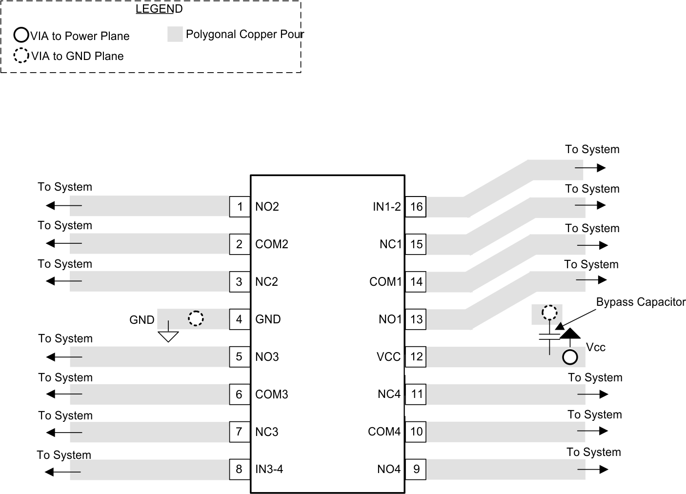 Figure 30. PCB Layout Example