JAJSG58G January 2005 – January 2019 TS3A5017
PRODUCTION DATA.
- 1 特長
- 2 アプリケーション
- 3 概要
- 4 改訂履歴
- 5 Pin Configuration and Functions
-
6 Specifications
- 6.1 Absolute Maximum Ratings
- 6.2 ESD Ratings
- 6.3 Recommended Operating Conditions
- 6.4 Thermal Information
- 6.5 Electrical Characteristics for 3.3-V Supply
- 6.6 Electrical Characteristics for 2.5-V Supply
- 6.7 Switching Characteristics for 3.3-V supply
- 6.8 Switching Characteristics for 2.5-V supply
- 6.9 Typical Characteristics
- 7 Parameter Measurement Information
- 8 Detailed Description
- 9 Application and Implementation
- 10Power Supply Recommendations
- 11Layout
- 12デバイスおよびドキュメントのサポート
- 13メカニカル、パッケージ、および注文情報
パッケージ・オプション
デバイスごとのパッケージ図は、PDF版データシートをご参照ください。
メカニカル・データ(パッケージ|ピン)
- PW|16
- DBQ|16
- RGY|16
- D|16
- DGV|16
- RSV|16
サーマルパッド・メカニカル・データ
- RGY|16
発注情報
6.9 Typical Characteristics
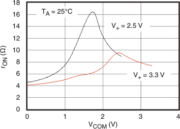 Figure 1. ron vs VCOM
 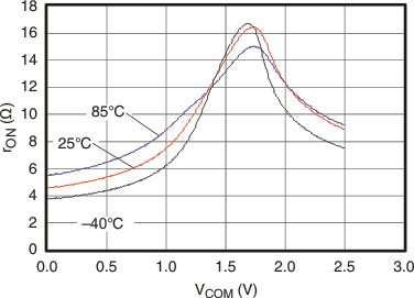 Figure 3. ron vs VCOM (V+ = 2.5 V)
 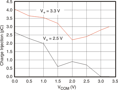 Figure 5. Charge Injection (QC) vs VCOM
 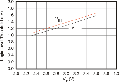 Figure 7. Logic-Level Threshold vs V+
 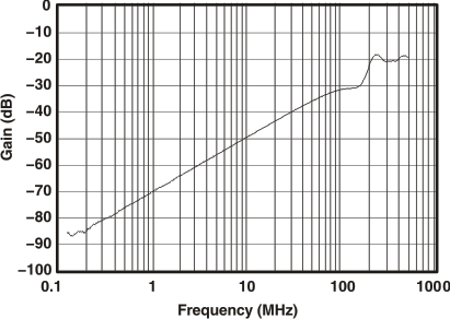 Figure 9. OFF Isolation and Crosstalk vs Frequency
(V+ = 3.3 V)
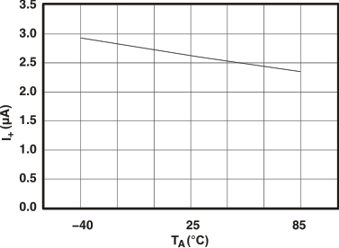 Figure 11. Power-Supply Current vs Temperature
(V+ = 3.6 V)
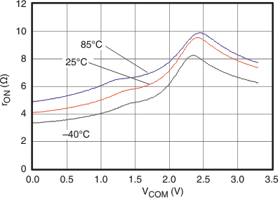 Figure 2. ron vs VCOM (V+ = 3.3 V)
 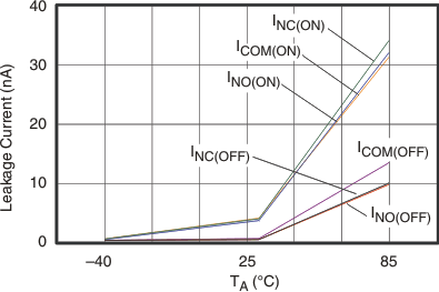 Figure 4. Leakage Current vs Temperature (V+ = 3.6 V)
 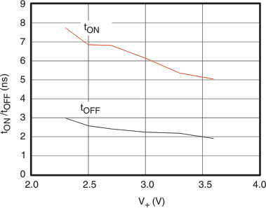 Figure 6. tON and tOFF vs Supply Voltage
 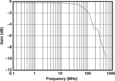 Figure 8. Bandwidth (Gain vs Frequency) (V+ = 3.3 V)
 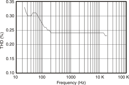 Figure 10. Total Harmonic Distortion vs Frequency