SWCS076B December 2011 – August 2014 TWL6032
UNLESS OTHERWISE NOTED, this document contains PRODUCTION DATA.
1 Device Overview
1.1 Features
-
Five Highly Efficient Buck Converters
- One 3 MHz, 0.6 to 2.1 V at 5.0 A, DVS-Capable
- One 6 MHz, 0.6 to 2.1 V at 2.5 A, DVS-Capable
- Three 6 MHz, 0.6 to 2.1 V at 1.1 A, One Is DVS-Capable
- Extended Mode for Higher Output Voltages
- 11 General-Purpose Low-Dropout Voltage Regulators (LDOs)
- Six 1.0 to 3.3 V at 0.2 A With Battery or Preregulated Supply:
- One Can be Used as Vibrator Driver
- One 1.0 to 3.3 V at 50 mA With Battery or Preregulated Supply
- One Low-Noise 1.0 to 3.3 V at 50 mA With Battery or Preregulated Supply
- One 3.3 V at 100 mA USB LDO
- Two LDOs for TWL6032 Internal Use
- Six 1.0 to 3.3 V at 0.2 A With Battery or Preregulated Supply:
- USB OTG Module:
- ID Detection, Accessory Charger Adapter (ACA) Support
- Accessory Detection Protocol (ADP) Support
- Backup Battery Charger
- 12-Bit Sigma-Delta Analog-to-Digital Converter (ADC) With 19 Input Channels:
- Seven External Input Channels
- 13-Bit Coulomb Counter With Four Programmable Integration Periods
- Low-Power Consumption:
- 8 µA in BACKUP State
- 20 µA in WAIT-ON State
- 110 µA in SLEEP State, With Two DC-DC Converters Active
- Real-Time Clock (RTC) With Timer and Alarm Wake-Up:
- Three Buffered 32-kHz Outputs
- SIM and SD/MMC Card Detections
- Two Digital PWM Outputs
- Thermal Monitoring:
- High-Temperature Warning
- Thermal Shutdown
- Control:
- Configurable Power-Up and Power-Down Sequences (OTP Memory)
- Configurable Sequences Between SLEEP and ACTIVE States (OTP Memory)
- Three Digital Output Signals that can be Included in the Startup Sequence to Control External Devices
- Two Inter-Integrated Circuit (I2C) Interfaces
- All Resources Configurable by I2C
- System Voltage Regulator and Battery Charger With Power Path From USB:
- Input Current Limit to Comply With USB Standard
- 3-MHz Switched-Mode Regulator With Integrated Power FET for up to 2.0-A Current
- Dedicated Control Loop for Battery Current and Voltage
- External Low-Ohmic FET for Power Path and Battery Charging
- Boost Mode Operation for USB OTG
- Supplement Mode to Deliver Current From Battery During Power Path Operation
- Charger for Single-Cell Li-Ion and Li-Polymer Battery Packs
- Safety Timer and Reset Control
- Thermal Protection
- Input/Output Overvoltage Protection
- Charging Indicator LED Driver
- Compliant With:
- USB 2.0
- OTG and EH 2.0
- USB Battery Charging 1.2
- YD/T 1591-2006
- Japanese Battery Charging Guidelines (JEITA)
- Battery Voltage Range From 2.5 to 5.5 V
- Package 5.21-mm × 5.36-mm 155-Pin WCSP
1.2 Applications
- Mobile Phones and Smart Phones
- Tablets
- Gaming Handsets
- Portable Media Players
- Portable Navigation Systems
- Handheld Devices
1.3 Description
The TWL6032 device is an integrated power-management integrated circuit (PMIC) for applications powered by a rechargeable battery. The device provides five configurable step-down converters with a current capability of up to 5.0 A for memory, processor core, I/O, auxiliary, preregulation for LDOs, and so forth. The device also contains nine LDO regulators for external use that can be supplied from a battery or a preregulated supply. The power-up and power-down controller is configurable and can support any power-up or power-down sequence (programmed in OTP memory). The RTC provides three 32-kHz clock outputs: seconds, minutes, hours, day, month, and year information; as well as alarm wakeup and timer. The TWL6032 device supports 32-kHz clock generation based on a crystal oscillator.
The device integrates a switched-mode system supply regulator from a USB connector. The switched-mode regulator includes power paths from the USB and battery with supplemental mode for immediate startup, even with an empty battery. The battery switch uses an external low-ohmic PMOS transistor allowing minimal serial resistance during fast charging and when operating from battery. The device can also be used without the external PMOS transistor; in this case, the battery is always tied to the system supply and the switched-mode regulator is used for battery charging.
The TWL6032 device is available in a 155-pin WCSP package, 5.21 mm × 5.36 mm with a 0.4-mm ball pitch.
Figure 1-1 shows the TWL6032 device block diagram.
1.4 Functional Block Diagram
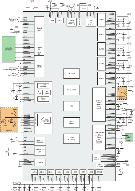 Figure 1-1 TWL6032 Device Block Diagram
For the complete TWL6032 data sheet (SWCS057), contact your TI sales representative.