SLUS794F November 2007 – April 2016 UCC28070
PRODUCTION DATA.
- 1 Features
- 2 Applications
- 3 Description
- 4 Revision History
- 5 Pin Configuration and Functions
- 6 Specifications
-
7 Detailed Description
- 7.1 Overview
- 7.2 Functional Block Diagram
- 7.3
Feature Description
- 7.3.1 Interleaving
- 7.3.2 Programming the PWM Frequency and Maximum Duty-Cycle Clamp
- 7.3.3 Frequency Dithering (Magnitude and Rate)
- 7.3.4 External Clock Synchronization
- 7.3.5 Multi-phase Operation
- 7.3.6 VSENSE and VINAC Resistor Configuration
- 7.3.7 VSENSE and VINAC Open-Circuit Protection
- 7.3.8 Current Synthesizer
- 7.3.9 Programmable Peak Current Limit
- 7.3.10 Linear Multiplier and Quantized Voltage Feed Forward
- 7.3.11 Enhanced Transient Response (VA Slew-Rate Correction)
- 7.3.12 Voltage Biasing (VCC and VVREF)
- 7.3.13 PFC Enable and Disable
- 7.3.14 Adaptive Soft Start
- 7.3.15 PFC Start-Up Hold Off
- 7.3.16 Output Overvoltage Protection (OVP)
- 7.3.17 Zero-Power Detection
- 7.3.18 Thermal Shutdown
- 7.3.19 Current Loop Compensation
- 7.3.20 Voltage Loop Compensation
- 7.4 Device Functional Modes
-
8 Application and Implementation
- 8.1 Application Information
- 8.2
Typical Application
- 8.2.1 Design Requirements
- 8.2.2
Detailed Design Procedure
- 8.2.2.1 Output Current Calculation
- 8.2.2.2 Bridge Rectifier
- 8.2.2.3 PFC Inductor (L1 and L2)
- 8.2.2.4 PFC MOSFETs (M1 and M2)
- 8.2.2.5 PFC Diode
- 8.2.2.6 PFC Output Capacitor
- 8.2.2.7 Current Loop Feedback Configuration (Sizing of the Current Transformer Turns Ratio and Sense Resistor (RS)
- 8.2.2.8 Current Sense Offset and PWM Ramp for Improved Noise Immunity
- 8.2.3 Application Curves
- 9 Power Supply Recommendations
- 10Layout
- 11Device and Documentation Support
- 12Mechanical, Packaging, and Orderable Information
1 Features
- Interleaved Average Current-Mode PWM Control With Inherent Current Matching
- Advanced Current Synthesizer Current Sensing for Superior Efficiency
- Highly-Linear Multiplier Output With Internal Quantized Voltage Feed-Forward Correction for Near-Unity PF
- Programmable Frequency from 30 kHz to 300 kHz
- Programmable Maximum Duty-Cycle Clamp
- Programmable Frequency-Dithering Rate and Magnitude for Enhanced EMI Reduction
- Magnitude: 3 kHz to 30 kHz
- Rate: Up to 30 kHz
- External-Clock Synchronization Capability
- Enhanced Load and Line Transient Response through Voltage Amplifier Output Slew-Rate Correction
- Programmable Peak Current Limiting
- Bias-Supply UVLO, Overvoltage Protection, Open-Loop Detection, and PFC-Enable Monitoring
- External PFC-Disable Interface
- Open-Circuit Protection on VSENSE and VINAC pins
- Programmable Soft-Start
2 Applications
- High-Efficiency Server and Desktop Power Supplies
- Telecom Rectifiers
- White Goods and Industrial Equipment
3 Description
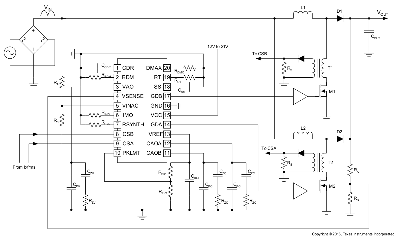
The UCC28070 is an advanced power factor correction (PFC) device that integrates two pulse-width modulators (PWMs) operating 180° out of phase. This interleaved PWM operation generates substantial reduction in the input and output ripple currents, allowing the conducted-EMI filtering to become easier and less expensive. A significantly improved multiplier design provides a shared current reference to two independent current amplifiers that ensures matched average-current mode control in both PWM outputs while maintaining a stable, low-distortion, sinusoidal input-line current.
The UCC28070 device contains multiple innovations including current synthesis and quantized voltage feed-forward to promote performance enhancements in PF, efficiency, THD, and transient response. Features including frequency dithering, clock synchronization, and slew rate enhancement further expand the potential performance enhancements.
The UCC28070 device also contains a variety of protection features including output-overvoltage detection, programmable peak-current limit, undervoltage lockout, and open-loop protection.
Device Information(1)
| PART NUMBER | PACKAGE | BODY SIZE (NOM) |
|---|---|---|
| UCC28070DW | SOIC (20) | 12.80 mm × 7.50 mm |
| UCC28070DWR | SOIC (20) | 12.80 mm × 7.50 mm |
| UCC28070PW | TSSOP (20) | 6.50 mm × 4.40 mm |
| UCC28070PWG4 | TSSOP (20) | 6.50 mm × 4.40 mm |
| UCC28070PWR | TSSOP (20) | 6.50 mm × 4.40 mm |
| UCC28070PWRG4 | TSSOP (20) | 6.50 mm × 4.40 mm |
- For all available packages, see the orderable addendum at the end of the data sheet.
Simplified Application Diagram
