JAJSE40A October 2017 – February 2018 UCC28780
PRODUCTION DATA.
- 1 特長
- 2 アプリケーション
- 3 概要
- 4 改訂履歴
- 5 Pin Configuration and Functions
- 6 Specifications
-
7 Detailed Description
- 7.1 Overview
- 7.2 Functional Block Diagram
- 7.3
Detailed Pin Description
- 7.3.1 BUR Pin (Programmable Burst Mode)
- 7.3.2 FB Pin (Feedback Pin)
- 7.3.3 VDD Pin (Device Bias Supply)
- 7.3.4 REF Pin (Internal 5-V Bias)
- 7.3.5 HVG and SWS Pins
- 7.3.6 RTZ Pin (Sets Delay for Transition Time to Zero)
- 7.3.7 RDM Pin (Sets Synthesized Demagnetization Time for ZVS Tuning)
- 7.3.8 RUN Pin (Driver Enable Pin)
- 7.3.9 SET Pin
- 7.4
Device Functional Modes
- 7.4.1 Adaptive ZVS Control with Auto-Tuning
- 7.4.2 Dead-Time Optimization
- 7.4.3 Control Law across Entire Load Range
- 7.4.4 Adaptive Amplitude Modulation (AAM)
- 7.4.5 Adaptive Burst Mode (ABM)
- 7.4.6 Low Power Mode (LPM)
- 7.4.7 Standby Power Mode (SBP)
- 7.4.8 Startup Sequence
- 7.4.9 Survival Mode of VDD
- 7.4.10 System Fault Protections
- 7.4.11 Pin Open/Short Protections
-
8 Application and Implementation
- 8.1 Application Information
- 8.2
Typical Application Circuit
- 8.2.1 Design Requirements
- 8.2.2 Detailed Design Procedure
- 8.2.3 Application Curves
- 9 Power Supply Recommendations
- 10Layout
- 11デバイスおよびドキュメントのサポート
- 12メカニカル、パッケージ、および注文情報
パッケージ・オプション
デバイスごとのパッケージ図は、PDF版データシートをご参照ください。
メカニカル・データ(パッケージ|ピン)
- D|16
- RTE|16
サーマルパッド・メカニカル・データ
- RTE|16
発注情報
7.4.3 Control Law across Entire Load Range
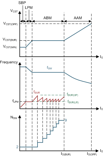
UCC28780 contains four modes of operation summarized in Table 1. Starting from heavier load, the AAM mode forces PWML and PWMH into complementary switching with ZVS tuning enabled. ABM mode generates a group of PWML and PWMH pulses as a burst packet, and adjusts the burst off-time to regulate the output voltage. At the same time, the burst frequency variation is confined above 20kHz by adjusting the number of PWML and PWMH pulses per packet to mitigate audible noise and reduce burst output ripple. In LPM and SBP modes, PWMH and the ZVS tuning loop are disabled, so the converter operates in valley-switching.
Table 1. Functional Modes
| MODE | OPERATION | PWMH | ZVS | |
|---|---|---|---|---|
| AAM | Adaptive Amplitude Modulation | ACF operation with PWML and PWMH in complementary switching | Enabled | Yes |
| ABM | Adaptive Burst Mode | Variable fBUR > 20 kHz, ACF operation in complementary switching | Enabled | Yes |
| LPM | Low Power Mode | Fix fBUR ≈ 25 kHz, valley-switching | Disabled | No |
| SBP | StandBy Power | Variable fBUR < 25 kHz, valley-switching | Disabled | No |
Figure 23 addresses the critical parameter changes among the four operating modes, where VCST is the peak current threshold compared with the current-sense voltage from CS pin, fSW is the switching frequency of PWML, fBUR is the burst frequency, and NSW is the pulse number of PWML per burst packet. The following section explains the detailed operation of each mode.
 Figure 23. Control Law Over Entire Load Range