JAJSE40A October 2017 – February 2018 UCC28780
PRODUCTION DATA.
- 1 特長
- 2 アプリケーション
- 3 概要
- 4 改訂履歴
- 5 Pin Configuration and Functions
- 6 Specifications
-
7 Detailed Description
- 7.1 Overview
- 7.2 Functional Block Diagram
- 7.3
Detailed Pin Description
- 7.3.1 BUR Pin (Programmable Burst Mode)
- 7.3.2 FB Pin (Feedback Pin)
- 7.3.3 VDD Pin (Device Bias Supply)
- 7.3.4 REF Pin (Internal 5-V Bias)
- 7.3.5 HVG and SWS Pins
- 7.3.6 RTZ Pin (Sets Delay for Transition Time to Zero)
- 7.3.7 RDM Pin (Sets Synthesized Demagnetization Time for ZVS Tuning)
- 7.3.8 RUN Pin (Driver Enable Pin)
- 7.3.9 SET Pin
- 7.4
Device Functional Modes
- 7.4.1 Adaptive ZVS Control with Auto-Tuning
- 7.4.2 Dead-Time Optimization
- 7.4.3 Control Law across Entire Load Range
- 7.4.4 Adaptive Amplitude Modulation (AAM)
- 7.4.5 Adaptive Burst Mode (ABM)
- 7.4.6 Low Power Mode (LPM)
- 7.4.7 Standby Power Mode (SBP)
- 7.4.8 Startup Sequence
- 7.4.9 Survival Mode of VDD
- 7.4.10 System Fault Protections
- 7.4.11 Pin Open/Short Protections
-
8 Application and Implementation
- 8.1 Application Information
- 8.2
Typical Application Circuit
- 8.2.1 Design Requirements
- 8.2.2 Detailed Design Procedure
- 8.2.3 Application Curves
- 9 Power Supply Recommendations
- 10Layout
- 11デバイスおよびドキュメントのサポート
- 12メカニカル、パッケージ、および注文情報
パッケージ・オプション
デバイスごとのパッケージ図は、PDF版データシートをご参照ください。
メカニカル・データ(パッケージ|ピン)
- D|16
- RTE|16
サーマルパッド・メカニカル・データ
- RTE|16
発注情報
7.4.10.2 Output Over-Voltage Protection
VS pin senses the positive voltage level of the auxiliary winding voltage (VAUX) to detect an over-voltage condition of VO. When an OVP event is triggered, UCC28780 stops switching and there is a 1.5-s fault recovery time (tFDR) before any VO restart attempt is made. As QL turns off, the settled VAUX is equal to (VO+VF) x NAS, where NAS is the auxiliary-to-secondary turns ratio of the transformer, NA / NS, and VF is the forward voltage drop of the secondary-side rectifier. The VS pin senses VAUX through a voltage divider formed by RVS1 and RVS2. The pin voltage (VVS) is compared with an internal OVP threshold (VOVP). If VVS ≥ VOVP condition is qualified for three consecutive PWML pulses, the controller stops switching, brings RUN pin low, and initiates the 1.5-s time delay. During this long delay time, only the UVLO-cycle of VVDD is active, and there are no test pulses of PWML. After the 1.5-s timeout is completed and VVDD reaches the next VVDD(OFF), a normal start sequence begins. The calculation of RVS2 is

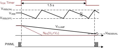
The long tFDR timer helps to protect the power stage components from the large current stress during every restart. After OVP is triggered, VO may be brought down quickly by the output load current. If OVP were reset directly after one UVLO cycle of VDD without the 1.5-s delay, the first PWMH pulse turns on QH under the condition of a large voltage difference between the high clamp capacitor voltage (VCLAMP) and the low reflected voltage. A large current can flow through the clamp switch (QH) and secondary rectifier. Therefore, the 1.5-s timer of UCC28780 allows VCLAMP to drop to a lower voltage level through a bleeding resistor (RBLEED) in parallel with CCLAMP before the next VO restart attempt, such that the current stress can be minimized. A large RBLEED can be used with the long time-out to minimize the impact on standby power. For example, to discharge VCLAMP to 10% of its normal level in 1.5 s, only 3 mW of additional standby power is added with RBLEED = 2.8 MΩ and CCLAMP = 220 nF. Figure 32 illustrates the timing sequence as VCLAMP is discharged to a residual voltage (VRESIDUAL) in 1.5 s. RBLEED also helps to reduce the voltage overcharge on the clamp capacitor in LPM and SBP modes in which PWMH is disabled, so the voltage stress in the passive-clamp operation can be controlled.
During LPM to ABM mode transition, it is possible to falsely trigger OVP if the setting does not have enough design margin. In LPM mode with a disabled PWMH, the leakage energy of the transformer charges VCLAMP higher than the reflected voltage. When the controller enters into ABM and the PWMH is enabled, the active-clamp circuit of ACF needs to take some time to balance the voltage difference, depending on the clamp capacitor value. As a result, VAUX can sense the higher VCLAMP condition during the voltage balancing and the controller may treat this as an OVP event, even though VO still stays in regulation and does not reach the actual OVP point. It may only happen with a large CCLAMP design, so slightly increasing the OVP setting can resolve the problem.
 Figure 32. Timing Diagram of CCLAMP Discharging During 1.5-s Recovery Time