JAJSE40A October 2017 – February 2018 UCC28780
PRODUCTION DATA.
- 1 特長
- 2 アプリケーション
- 3 概要
- 4 改訂履歴
- 5 Pin Configuration and Functions
- 6 Specifications
-
7 Detailed Description
- 7.1 Overview
- 7.2 Functional Block Diagram
- 7.3
Detailed Pin Description
- 7.3.1 BUR Pin (Programmable Burst Mode)
- 7.3.2 FB Pin (Feedback Pin)
- 7.3.3 VDD Pin (Device Bias Supply)
- 7.3.4 REF Pin (Internal 5-V Bias)
- 7.3.5 HVG and SWS Pins
- 7.3.6 RTZ Pin (Sets Delay for Transition Time to Zero)
- 7.3.7 RDM Pin (Sets Synthesized Demagnetization Time for ZVS Tuning)
- 7.3.8 RUN Pin (Driver Enable Pin)
- 7.3.9 SET Pin
- 7.4
Device Functional Modes
- 7.4.1 Adaptive ZVS Control with Auto-Tuning
- 7.4.2 Dead-Time Optimization
- 7.4.3 Control Law across Entire Load Range
- 7.4.4 Adaptive Amplitude Modulation (AAM)
- 7.4.5 Adaptive Burst Mode (ABM)
- 7.4.6 Low Power Mode (LPM)
- 7.4.7 Standby Power Mode (SBP)
- 7.4.8 Startup Sequence
- 7.4.9 Survival Mode of VDD
- 7.4.10 System Fault Protections
- 7.4.11 Pin Open/Short Protections
-
8 Application and Implementation
- 8.1 Application Information
- 8.2
Typical Application Circuit
- 8.2.1 Design Requirements
- 8.2.2 Detailed Design Procedure
- 8.2.3 Application Curves
- 9 Power Supply Recommendations
- 10Layout
- 11デバイスおよびドキュメントのサポート
- 12メカニカル、パッケージ、および注文情報
パッケージ・オプション
デバイスごとのパッケージ図は、PDF版データシートをご参照ください。
メカニカル・データ(パッケージ|ピン)
- D|16
- RTE|16
サーマルパッド・メカニカル・データ
- RTE|16
発注情報
7.4.10.3 Over-Temperature Protection
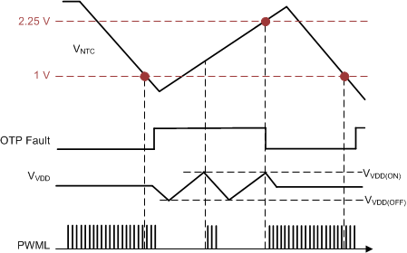
The UCC28780 uses an external NTC resistor (RNTC) tied to the NTC pin to program a thermal shutdown temperature near the hotspot of the converter. The NTC shutdown threshold (VNTCTH) of 1 V with an internal 105-μA current source flowing through RNTC results in a 9.5-kΩ thermistor shutdown threshold. If the NTC resistance stays lower than 9.5 kΩ for more than three consecutive PWML pulses, an OTP fault event is triggered, and the 1-V threshold is increased to 2.25 V. The NTC resistance has to increase above 21.7 kΩ to reset the OTP fault. This threshold change provides a safe temperature hysteresis to help the hot-spot temperature cool down before the next VO restart attempt, reducing the thermal stress to the components. This pin can also be used as an electrical shutdown function by shorting this pin with a controlled switch to GND. With the pin shorted to GND, VVDD performs UVLO cycling, and there is at least three consecutive PWML pulses generated to check the state. The NTC pin can be left floating or tied to the REF pin if not used.
 Figure 33. Timing Diagram of OTP with NTC