JAJSE40A October 2017 – February 2018 UCC28780
PRODUCTION DATA.
- 1 特長
- 2 アプリケーション
- 3 概要
- 4 改訂履歴
- 5 Pin Configuration and Functions
- 6 Specifications
-
7 Detailed Description
- 7.1 Overview
- 7.2 Functional Block Diagram
- 7.3
Detailed Pin Description
- 7.3.1 BUR Pin (Programmable Burst Mode)
- 7.3.2 FB Pin (Feedback Pin)
- 7.3.3 VDD Pin (Device Bias Supply)
- 7.3.4 REF Pin (Internal 5-V Bias)
- 7.3.5 HVG and SWS Pins
- 7.3.6 RTZ Pin (Sets Delay for Transition Time to Zero)
- 7.3.7 RDM Pin (Sets Synthesized Demagnetization Time for ZVS Tuning)
- 7.3.8 RUN Pin (Driver Enable Pin)
- 7.3.9 SET Pin
- 7.4
Device Functional Modes
- 7.4.1 Adaptive ZVS Control with Auto-Tuning
- 7.4.2 Dead-Time Optimization
- 7.4.3 Control Law across Entire Load Range
- 7.4.4 Adaptive Amplitude Modulation (AAM)
- 7.4.5 Adaptive Burst Mode (ABM)
- 7.4.6 Low Power Mode (LPM)
- 7.4.7 Standby Power Mode (SBP)
- 7.4.8 Startup Sequence
- 7.4.9 Survival Mode of VDD
- 7.4.10 System Fault Protections
- 7.4.11 Pin Open/Short Protections
-
8 Application and Implementation
- 8.1 Application Information
- 8.2
Typical Application Circuit
- 8.2.1 Design Requirements
- 8.2.2 Detailed Design Procedure
- 8.2.3 Application Curves
- 9 Power Supply Recommendations
- 10Layout
- 11デバイスおよびドキュメントのサポート
- 12メカニカル、パッケージ、および注文情報
パッケージ・オプション
デバイスごとのパッケージ図は、PDF版データシートをご参照ください。
メカニカル・データ(パッケージ|ピン)
- D|16
- RTE|16
サーマルパッド・メカニカル・データ
- RTE|16
発注情報
5 Pin Configuration and Functions
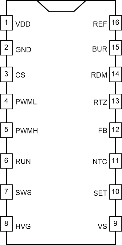
D Package
16-Pin SOIC
Top View

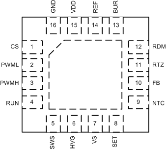
RTE Package
16-Pin WQFN
Top View

Pin Functions
| PIN | TYPE(1) | DESCRIPTION | ||
|---|---|---|---|---|
| NAME | SOIC | WQFN | ||
| BUR | 15 | 13 | I | This pin is used to program the burst level of the converter at light load. A resistive divider between REF and GND is used to set a voltage at this pin to determine the peak current level when the converter enters the adaptive burst mode. In addition, the Thevenin resistance on BUR pin (equivalent resistance of the divider resistors in parallel) is used to set an offset voltage for smooth mode transition which increases the peak current level when the converter enters the low power mode. |
| CS | 3 | 1 | I | This is the current sense input pin. This pin couples through a line-compensation resistor to a current-sense resistor to sense and control the peak primary current in each switching cycle. A current sourced from this pin, which magnitude is proportional to the converter’s input voltage derived from the VS-pin input signal, creates an offset voltage across the line-compensation resistor to program an OPP level at high line. |
| FB | 12 | 10 | I | The feedback current signal to close the converter’s regulation loop is coupled to this pin. This pin presents a 4-V output that is designed to have 0-µA to 75-µA current pulled out of the pin corresponding to the converter operating from full-power to zero-power conditions. |
| GND | 2 | 16 | G | Ground reference and return for all controller signals. |
| HVG | 8 | 6 | O | The high-voltage gate pin is used to control the gate of an external depletion-mode MOSFET for start-up and switch-node voltage sensing. A 2.2-nF ceramic bypass capacitor to ground is required. |
| NTC | 11 | 9 | I | This is an interface to an external NTC (negative temperature coefficient) thermistor for remote temperature sensing. Pulling this pin low shuts down PWM action and initiates a fault response. |
| PWMH | 5 | 3 | O | The PWMH pin is a logic-level output signal used to control the gate of the high-side clamp switch through an external gate driver. |
| PWML | 4 | 2 | O | The PWML pin is a logic-level output signal used to control the gate of the low-side primary switch through an external gate driver. |
| RDM | 14 | 12 | I | A resistor to ground on this pin programs a synthesized demagnetization time used to control the on-time of the high-side switch to achieve zero voltage switching on the low-side switch. The controller applies a voltage on this pin that varies with the output voltage derived from the VS pin signal. |
| REF | 16 | 14 | O | 5V reference output that requires a 0.1-µF ceramic bypass capacitor to ground. This reference is used to power internal circuits and can supply a limited external load current. |
| RTZ | 13 | 11 | I | A resistor to ground on this pin programs an adaptive transition-to-zero delay from the turn-off edge of the high-side clamp switch to the turn-on edge of the low-side switch. |
| RUN | 6 | 4 | O | This output pin is high when the controller is in a run state. During start-up and wait states this output is low. It can be used to enable and disable the external gate drivers to reduce the static power consumption. There is a preset delay, tD(RUN-PWML), of about 2.2 µs that delays the initiation of PWML switching after this pin has gone high. |
| SET | 10 | 8 | I | This pin is used to configure the controller to be optimized for Gallium Nitride (GaN) power FETs or silicon (Si) power FETs on the primary side. Depending on setting, it will optimize parameters of the ZVS control loop, dead-time adjustment, and protection features. When pulled high to REF pin, it is optimized for Si FETs. When pulled low to GND, it is optimized for GaN FETs . |
| SWS | 7 | 5 | I | This sensing input is used to monitor the switch-node voltage as it nears zero volts in normal operation. During start-up, this pin is connected to the VDD pin internally to allow the high-voltage sensing network to provide start-up current. |
| VDD | 1 | 15 | P | Bias power input to the controller. A hold-up capacitor to ground is required for the bias power supplied from the transformer auxiliary winding to this pin. |
| VS | 9 | 7 | I | This voltage sensing input pin is coupled to the auxiliary winding of the converter’s transformer via a resistor divider. The pin and the associated external resistors are used to monitor the output and input voltages of the converter. |
(1) I = Input, O = Output, P = Power, G = Ground