SLUSC05D July 2014 – May 2016 UCC28880
PRODUCTION DATA.
- 1 Features
- 2 Applications
- 3 Description
- 4 Revision History
- 5 Pin Configuration and Functions
- 6 Specifications
- 7 Detailed Description
-
8 Application and Implementation
- 8.1 Application Information
- 8.2
Typical Application
- 8.2.1
12-V, 100-mA Low-Side Buck Converter
- 8.2.1.1 Design Requirements
- 8.2.1.2
Detailed Design Procedure
- 8.2.1.2.1 Custom Design with WEBENCH Tools
- 8.2.1.2.2 Input Stage (RF, D2, D3, C1, C2, L2)
- 8.2.1.2.3 Regulator Capacitor (CVDD)
- 8.2.1.2.4 Freewheeling Diode (D1)Freewheeling Diode (D1) section.
- 8.2.1.2.5 Output Capacitor (CL)
- 8.2.1.2.6 Load Resistor (RL)
- 8.2.1.2.7 Inductor (L1)
- 8.2.1.2.8 Feedback Path (Q1, RFB1, RFB2)
- 8.2.1.3 Application Curves
- 8.2.2 12-V, 100-mA, High-Side Buck Converter
- 8.2.3 Additional UCC28880 Application Topologies
- 8.2.1
12-V, 100-mA Low-Side Buck Converter
- 9 Power Supply Recommendations
- 10Layout
- 11Device and Documentation Support
- 12Mechanical, Packaging, and Orderable Information
7 Detailed Description
7.1 Overview
The UCC28880 integrates a controller and a 700-V power MOSFET into one monolithic device. The device also integrates a high-voltage current source, enabling start up and operation directly from the rectified mains voltage.
The low-quiescent current of the device enables excellent efficiency. The device is suitable for non-isolated AC-to-DC low-side buck and buck-boost configurations with level-shifted direct feedback, but also more traditional high-side buck, buck boost and low-power flyback converters with low standby power can be built using a minimum number of external components.
The device generates its own internal low-voltage supply (5 V referenced to the device’s ground, GND) from the integrated high-voltage current source. The PWM signal generation is based on a maximum constant on-time, minimum off-time concept, with the triggering of the on-pulse depending on the feedback voltage level. Each on-pulse is followed by a minimum off-time to ensure that the power MOSFET is not continuously driven in an on-state. The PWM signal is AND-gated with the signal from a current limit circuit. No internal clock is required, as the switching of the power MOSFET is load dependent. A special protection mechanism is included to avoid runaway of the inductor current when the converter operates with the output shorted or in other abnormal conditions that can lead to an uncontrolled increase of the inductor current. This special protection feature keeps the MOSFET current at a safe operating level. The device is also protected from other fault conditions with thermal shutdown, under-voltage lockout and soft-start features.
7.2 Functional Block Diagram
7.3 Feature Description
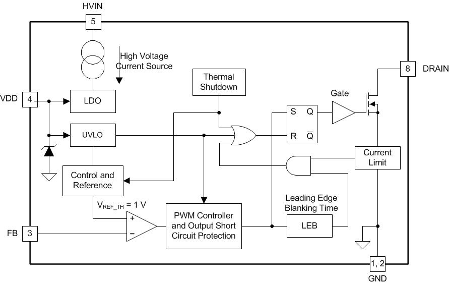
The device integrates a 700-V rated power MOSFET switch, a PWM controller, a high-voltage current source to supply a low-voltage power supply regulator, a bias and reference block, thermal shutdown and the following protection features, current limiter, under voltage lockout (UVLO) and overload protection for situations like short circuit at the output.
In low-side buck and buck-boost topologies, the external level-shifted direct feedback circuit can be implemented by two resistors and a high-voltage PNP transistor.
The positive high-voltage input of the converter node (VIN+) functions as a system reference ground for the output voltage in low-side topologies. In the low-side buck topology the output voltage is negative with respect to the positive high-voltage input (VIN+), and in low-side buck-boost topology the output voltage is positive with respect to the positive high-voltage input (VIN+).
In high-side buck configuration, as well as in non-isolated flyback configuration, the output voltage is positive with respect to the negative high-voltage input (VIN-), which is the system reference ground.
UCC28880 can operate under continuous conduction mode (CCM) or discontinuous conduction mode (DCM) mode. CCM operation allows the converter to deliver more output power because of less current ripple. However, it requires a higher inductor value and generally results in lower efficiency due to the added losses associated with diode reverse recovery current. On the other hand, DCM mode operation uses a smaller inductor and achieves better efficiency, but the output current handling capability is reduced because of increased current ripple. The table below shows the current handling capability in DCM and CCM operation.
Table 1. Current Handling Capability
| CURRENT HANDLING MODE | 230 VAC ±15% | 85 V ~ 265 VAC |
|---|---|---|
| Discontinuous Conduction Mode (DCM) | 70 mA | 70 mA |
| Continuous Conduction Mode (CCM) | 100 mA | 100 mA |
When the bus voltage is higher than 400 V, it is recommended to limit operation to DCM mode only to avoid the diode reverse recovery current and the associated internal MOSFET stress. Due to the higher switching loss and device stresses at higher bus voltage, it is recommended to keep the converter input voltage less than 560 V for the buck applications.
UCC28880 power handling capability is reduced at higher ambient temperature, as a function of the power dissipation of the device, the device's recommended maximum operating junction temperature and the thermal dissipation capability of the total system. De-rating of the output current according to maximum ambient temperature can be estimated from Figure 12. The de-rating estimation assumes CCM operation, 7 µJ of switching loss and 135°C/W RTHJA and 30-kHz full-load switching frequency. This is a conservative estimation. The thermal handling capability can be more accurately determined through experimental measurement. For more information on thermal evaluation methods see the IC Package and Thermal Metrics application report: SPRA953.
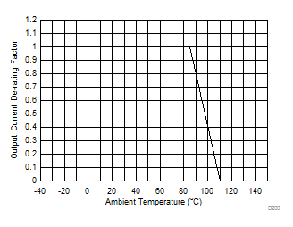 Figure 12. Output Current (De-Rating Factor) vs. Temperature
It is required to use fast recovery diode for the buck freewheeling diode. When designed in CCM, the diode reverse recovery time should be less than 35 ns to keep low reverse recovery current and the switching loss. For example, STTH1R06A provides 25-ns reverse recovery time. When designed in DCM, a slower diode can be used, but the reverse-recovery time should be kept less than 75 ns. MURS160 can fit the requirement.
The device has a low-standby power consumption (no-load condition), only 18 mW (typical) when connected to a 230-VAC mains and 9 mW when connected to an 115-VAC mains.
The standby power does not include the power dissipated in the external feedback path, the power dissipated in the external pre-load, the inductor in the freewheeling diode and the converter input stage (rectifiers and filter).
7.4 Device Functional Modes
7.4.1 Startup Operation
The device includes a high-voltage current source connected between the HVIN pin and the internal supply for the regulator. When the voltage on the HVIN pin rises, the current source is activated and starts to supply current to the internal 5-V regulator. The 5-V regulator charges the external capacitor connected between VDD pin and GND pin. When the VDD voltage exceeds the VDD turn-on threshold, VVDD(on), device starts operations. The minimum voltage across HVIN and GND pins, to ensure enough current to charge the capacitance on VDD pin, is VHVIN(min). At the First switching cycle the minimum MOSFET off time is set to be >100 μs and cycle-by-cycle is progressively reduced up to tOFF(min) providing soft start.
7.4.2 Feedback and Voltage Control Loop
The feedback circuit consists of a voltage comparator with the positive input connected to an internal reference voltage (referenced to GND) and the negative input connected to FB pin. When the feedback voltage at the FB pin is below the reference voltage VFB_TH logic high is generated at the comparator output. This logic high triggers the PWM controller, which generates the PWM signal turning on the MOSFET. When the feedback voltage at the FB pin is above the reference voltage, it indicates that the output voltage of the converter is above the targeted output voltage set by the external feedback circuitry and PWM is stopped.
7.4.3 PWM Controller
UCC28880 operates under on/off control. When the FB pin voltage is below internal reference 1 V, the converter is switching and sending power to the load. When the FB pin voltage is above internal reference 1 V, the converter shuts off and stops delivering power to the load.
The PWM controller does not need a clock signal. The PWM signal’s frequency is set to fSW(max) = (1/(tON(max) + tOFF(min))) which occurs when the voltage on the FB pin is continuously below VFB_TH.
PWM duty cycle is determined by both the peak current and maximum on time. At each switching cycle, after turn on, the MOSFET is turned off if its current reaches the fixed peak-current threshold or its on time reaches the maximum value of on-time pulse tON(max).
Normally the converter would operate under frequency control, which means the converter is only enabled one switching cycle and then disabled. Next switching cycle starts when output voltage decays and the feedback enable the converter again. This way, the converter appears to operate under variable switching frequency control.
The user might observe the converter operates in burst mode that converter is enabled for multiple switching cycles and then stopped for multiple switching cycles. This causes larger output voltage ripple. However, due to the infrequent switching it actually helps on the standby power at no load.
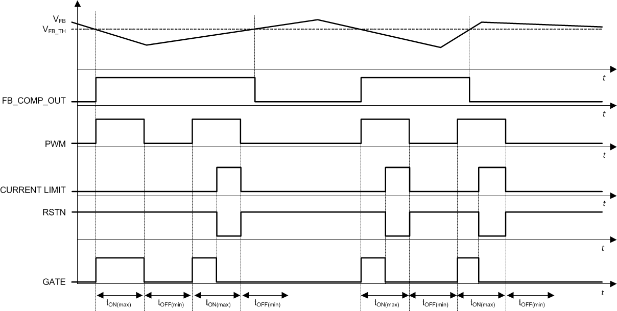 Figure 13. UCC28880 Timing Diagram
7.4.4 Current Limit
The current limit circuit senses the current through the power MOSFET. The sensing circuit is located between the source of the power MOSFET and the GND pin. When the current in the power MOSFET exceeds the threshold ILIMIT, the internal current limit signal goes high, which sets the internal RSTN signal low. This disables the power MOSFET by driving its gate low. The current limit signal is set back low after the falling edge of the PWM signal. After the rising edge of the GATE signal, there is a blanking time. During this blanking time, the current limit signal cannot go high. This blanking time and the internal propagation delay result in minimum on time, tMIN.
7.4.5 Inductor Current Runaway Protection
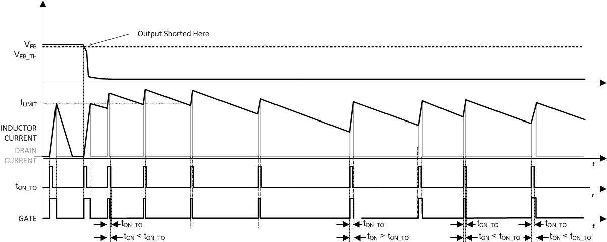
To protect the device from overload conditions, including a short circuit at the output, the PWM controller incorporates a protection feature which prevents the inductor current from runaway. When the output is shorted the inductor demagnetization is very slow, low di/dt, and when the next switching cycle starts energy stored in the inductance is still high. After the MOSFET switches on, the current starts to rise from pre-existing DC value and reaches the current-limit value in a short duration of time. Because of the intrinsic minimum on-time of the device the MOSFET on-time cannot be lower than tMIN, in an overload or output short circuit the energy inductance is not discharged sufficiently during MOSFET off-time, it is possible to lose control of the current leading to a runaway of the inductor current. To avoid this, if the on-time is less than tON_TO (tON_TO is a device internal time out), the controller increases the MOSFET off-time (tOFF). If the MOSFET on-time is longer than tON_TO then tOFF is decreased. The controller increases tOFF, cycle-by-cycle, through discrete steps until the on-time continues to stay below tON_TO. The tOFF is increased up to tOFF(ovl) after that, if the on-time is still below tON_TO the off-time is kept equal to tOFF(ovl). The controller decreases tOFF cycle-by-cycle until the on-time continues to stay above tON_TO up to tOFF(min). This mechanism prevents control loss of the inductor current and prevents over stress of the MOSFET (see typical waveforms in Figure 14 and Figure 15). At start up, the tOFF is set to tOFF(ovl) and reduced cycle-by-cycle (if the on-time is longer than tON_TO) up to tOFF(min) providing a soft start for the power stage.
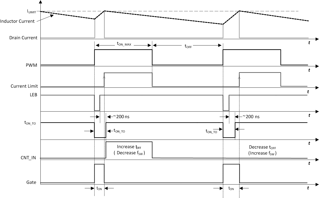 Figure 14. Current Runaway Protection Logic Timing Diagram
A minimal value needs to be imposed on the inductance value to avoid nuisance tripping of the protection feature that prevents the loss of control of the inductor current. Inadvertent operation of the protection feature limits the output-power capability of the converter. This condition depends on the converter's maximum input operating voltage and temperature. Use Equation 1 to calculate your minimum inductance value.
The value of Equation 1 can be found by characterization graph of Figure 10. Pick the value at the desired maximum junction temperature
If the inductance value is too low, such that the MOSFET on-time is always less than tON_TO timeout and the device progressively increases the MOSFET off-time up to tOFF(ovl), the output power is reduced and the converter fails to supply the load.
7.4.6 Thermal Shutdown
If the junction temperature rises above TJ(stop), the thermal shutdown is triggered. This disables the power MOSFET switching. To re-enable the switching of the MOSFET the junction temperature has to fall by TJ(hyst) below the TJ(stop) where the device moves out of over temperature.
According to the electrical specs, the thermal shutdown threshold can be beyond the device's rated absolute maximum junction temperature. Thermal shutdown is designed to prevent thermal run away that could result in catastrophic failure. Prolonged operation above the recommended maximum junction temperature can impact device lifetime.
