CD4541B
- Low Symmetrical Output Resistance, Typically 100
 at VDD = 15V
 - Built-In Low-Power RC Oscillator
- Oscillator Frequency Range . . . DC to 100kHz
- External Clock (Applied to Pin 3) can be Used Instead of Oscillator
- Operates as 2 N Frequency Divider or as a Single-Transition Timer
- Q/Q\ Select Provides Output Logic Level Flexibility
- AUTO or MASTER RESET Disables Oscillator During Reset to Reduce Power Dissipation
- Operates With Very Slow Clock Rise and Fall Times
- Capable of Driving Six Low Power TTL Loads, Three Low-Power Schottky Loads, or Six HTL Loads Over the Rated Temperature Range
- Symmetrical Output Characteristics
- 100% Tested for Quiescent Current at 20V
- 5V, 10V, and 15V Parametric Ratings
- Meets All Requirements of JEDEC Standard No. 13B, "Standard Specifications for Description of ’B’ Series CMOS Devices"
Data sheet acquired from Harris Semiconductor
CD4541B programmable timer consists of a 16-stage binary counter, an oscillator that is controlled by external R-C components (2 resistors and a capacitor), an automatic power-on reset circuit, and output control logic. The counter increments on positive-edge clock transitions and can also be reset via the MASTER RESET input.
The output from this timer is the Q or Q\ output from the 8th, 10th, 13th, or 16th counter stage. The desired stage is chosen using time-select inputs A and B (see Frequency Select Table).
The output is available in either of two modes selectable via the MODE input, pin 10 (see Truth Table). When this MODE input is a logic "1", the output will be a continuous square wave having a frequency equal to the oscillator frequency divided by 2N. With the MODE input set to logic "0" and after a MASTER RESET is initiated, the output (assuming Q output has been selected) changes from a low to a high state after 2N-1 counts and remains in that state until another MASTER RESET pulse is applied or the MODE input is set to a logic "1".
Timing is initialized by setting the AUTO RESET input (pin 5) to logic "0" and turning power on. If pin 5 is set to logic "1", the AUTO RESET circuit is disabled and counting will not start until after a positive MASTER RESET pulse is applied and returns to a low level. The AUTO RESET consumes an appreciable amount of power and should not be used if low-power operation is desired. For reliable automatic power-on reset, VDD should be greater than 5V.
The RC oscillator, shown in Figure 2, oscillates with a frequency determined by the RC network and is calculated using:
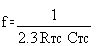 Where f is between 1kHz and 100kHz and RS and 2RTC.
技術資料
| 種類 | タイトル | 最新の英語版をダウンロード | 日付 | |||
|---|---|---|---|---|---|---|
| * | データシート | CD4541B データシート (Rev. E) | 2003年 8月 21日 | |||
| セレクション・ガイド | Logic Guide (Rev. AB) | 2017年 6月 12日 | ||||
| アプリケーション・ノート | Understanding and Interpreting Standard-Logic Data Sheets (Rev. C) | 2015年 12月 2日 | ||||
| セレクション・ガイド | ロジック・ガイド (Rev. AA 翻訳版) | 最新英語版 (Rev.AB) | 2014年 11月 6日 | |||
| ユーザー・ガイド | LOGIC Pocket Data Book (Rev. B) | 2007年 1月 16日 | ||||
| アプリケーション・ノート | Semiconductor Packing Material Electrostatic Discharge (ESD) Protection | 2004年 7月 8日 | ||||
| ユーザー・ガイド | Signal Switch Data Book (Rev. A) | 2003年 11月 14日 | ||||
| アプリケーション・ノート | Understanding Buffered and Unbuffered CD4xxxB Series Device Characteristics | 2001年 12月 3日 |
設計と開発
その他のアイテムや必要なリソースを参照するには、以下のタイトルをクリックして詳細ページをご覧ください。
14-24-LOGIC-EVM — 14 ピンから 24 ピンの D、DB、DGV、DW、DYY、NS、PW の各パッケージに封止した各種ロジック製品向けの汎用評価基板
14-24-logic-EVM 評価基板は、14 ピンから 24 ピンの D、DW、DB、NS、PW、DYY、DGV の各パッケージに封止した各種ロジック デバイスをサポートする設計を採用しています。
| パッケージ | ピン数 | ダウンロード |
|---|---|---|
| PDIP (N) | 14 | オプションの表示 |
| SOIC (D) | 14 | オプションの表示 |
| SOP (NS) | 14 | オプションの表示 |
| TSSOP (PW) | 14 | オプションの表示 |
購入と品質
- RoHS
- REACH
- デバイスのマーキング
- リード端子の仕上げ / ボールの原材料
- MSL 定格 / ピーク リフロー
- MTBF/FIT 推定値
- 材質成分
- 認定試験結果
- 継続的な信頼性モニタ試験結果
- ファブの拠点
- 組み立てを実施した拠点