SLAS837B April 2013 – January 2017 DAC3174
PRODUCTION DATA.
- 1 Features
- 2 Applications
- 3 Description
- 4 Revision History
- 5 Pin Configuration and Functions
-
6 Specifications
- 6.1 Absolute Maximum Ratings
- 6.2 ESD Ratings
- 6.3 Recommended Operating Conditions
- 6.4 Thermal Information
- 6.5 Electrical Characteristics: DC Specifications
- 6.6 Electrical Characteristics: AC Specifications
- 6.7 Electrical Characteristics: Digital Specifications
- 6.8 Timing Requirements
- 6.9 Typical Characteristics
-
7 Detailed Description
- 7.1 Overview
- 7.2 Functional Block Diagrams
- 7.3 Feature Description
- 7.4 Device Functional Modes
- 7.5 Programming
- 7.6
Register Maps
- 7.6.1 config0 Register (address = 0x00) [reset = 0x44FC]
- 7.6.2 config 1 Register (address = 0x01) [reset = 0x600E]
- 7.6.3 config2 Register (address = 0x02) [reset = 0x3FFF]
- 7.6.4 config3 Register (address = 0x03) [reset = 0x0000]
- 7.6.5 config4 Register (address = 0x04) [reset = 0x0000]
- 7.6.6 config5 Register (address = 0x05) [reset = 0x0000]
- 7.6.7 config6 Register (address = 0x06) [reset = 0x0000]
- 7.6.8 config7 Register (address = 0x07) [reset = 0xFFFF]
- 7.6.9 config8 Register (address = 0x08) [reset = 0x4000]
- 7.6.10 config9 Register (address = 0x09) [reset = 0x8000]
- 7.6.11 config10 Register (address = 0x0A) [reset = 0xF080]
- 7.6.12 config11 Register (address = 0x0B) [reset = 0x1111]
- 7.6.13 config12 Register (address = 0x0C) [reset = 0x3A7A]
- 7.6.14 config13 Register (address = 0x0D) [reset = 0x36B6]
- 7.6.15 config14 Register (address = 0x0E) [reset = 0x2AEA]
- 7.6.16 config15 Register (address = 0x0F) [reset = 0x0545]
- 7.6.17 config16 Register (address = 0x10) [reset = 0x0585]
- 7.6.18 config17 Register (address = 0x11) [reset = 0x0949]
- 7.6.19 config18 Register (address = 0x12) [reset = 0x1515]
- 7.6.20 config19 Register (address = 0x13) [reset = 0x3ABA]
- 7.6.21 config20 Register (address = 0x14) [reset = 0x0000]
- 7.6.22 config21 Register (address = 0x15) [reset = 0xFFFF]
- 7.6.23 config22 Register (address = 0x16) [reset = N/A]
- 7.6.24 config23 Register (address = 0x17) [reset = N/A]
- 7.6.25 config24 Register (address = 0x18) [reset = N/A]
- 7.6.26 config25 Register (address = 0x19) [reset = N/A]
- 7.6.27 config127 Register (address = 0x7F) [reset = 0x0045]
- 8 Application and Implementation
- 9 Power Supply Recommendations
- 10Layout
- 11Device and Documentation Support
- 12Mechanical, Packaging, and Orderable Information
パッケージ・オプション
メカニカル・データ(パッケージ|ピン)
- RGC|64
サーマルパッド・メカニカル・データ
- RGC|64
発注情報
1 Features
- Dual-Channel
- 14-Bit Resolution
- Maximum Sample Rate: 500 MSPS
- Pin Compatible With Dual-Channel DAC3154, DAC3164, and
Single-Channel DAC3151, DAC3161, and DAC3171 - Input Interface:
- 14 LVDS Inputs
- Single, 14-Bit Interface
or Dual, 7-Bit Interface - Single or Dual DDR Data Clock
- Internal FIFO
- Chip-to-Chip Synchronization
- Power Dissipation: 460 mW
- Spectral Performance at 20 MHz IF:
- SNR: 76 dBFS
- SFDR: 78 dBc
- Current-Sourcing DACs
- Compliance Range: –0.5 V to +1 V
- Package: 64-Pin VQFN (9 mm × 9 mm)
2 Applications
- Multi-Carrier, Multi-Mode Cellular Infrastructure Base Stations
- Radar
- Signal Intelligence
- Software-Defined Radios
- Test and Measurement Instrumentation
3 Description
The DAC3174 is a dual-channel, 14-bit, 500-MSPS, digital-to-analog converter (DAC). The DAC3174 uses a 14-bit, low-voltage differential signaling (LVDS) digital bus, with one or two independent dual-data rate (DDR) data clocks for flexibility in providing data from different sources in each channel.
An input first-in first out block (FIFO) allows independent data and sample clocks. FIFO input and output pointers can be synchronized across multiple devices for precise signal synchronization.
The DAC outputs are current sourcing and terminate to GND with a compliance range of –0.5 V to +1 V.
The DAC3174 is pin compatible with the dual-channel, 500-MSPS, 12-bit DAC3164 and 10-bit DAC3154, and the single-channel, 500-MSPS, 14-bit DAC3171, 12-bit DAC3161, and 10-bit DAC3151.
The device is available in a 64-pin VQFN PowerPAD™ package. and is specified over the full industrial temperature range of –40°C to +85°C.
Device Information(1)
| PART NUMBER | PACKAGE | BODY SIZE (NOM) |
|---|---|---|
| DAC3174 | VQFN (64) | 9.00 mm × 9.00 mm |
- For all available packages, see the package option addendum at the end of the data sheet.
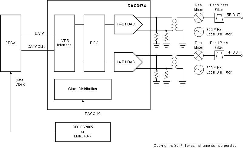
Typical Application
