SN75LVDS32
- Meets or Exceeds the Requirements of ANSI TIA/EIA-644 Standard
- Operates With a Single 3.3-V Supply
- Designed for Signaling Rate of up to 155 Mbps
- Differential Input Thresholds ±100 mV Max
- Low-Voltage TTL (LVTTL) Logic Output Levels
- Open-Circuit Fail Safe
- Characterized For Operation From 0&dg;C to 70°C
The SN75LVDS32 and SN75LVDS9637 are differential line receivers that implement the electrical characteristics of low-voltage differential signaling (LVDS). This signaling technique lowers the output voltage levels of 5-V differential standard levels (such as EIA/TIA-422B) to reduce the power, increase the switching speeds, and allow operation with a 3.3-V supply rail. Any of the four differential receivers provides a valid logical output state with a ±100 mV allow operation with a differential input voltage within the input common-mode voltage range. The input common-mode voltage range allows 1 V of ground potential difference between two LVDS nodes.
The intended application of these devices and signaling technique is both point-to-point and multidrop (one
driver and multiple receivers) data transmission over controlled impedance media of approximately 100  . The
transmission media may be printed-circuit board traces, backplanes, or cables. The ultimate rate and distance
of data transfer is dependent upon the attenuation characteristics of the media and the noise coupling to the
environment.
. The
transmission media may be printed-circuit board traces, backplanes, or cables. The ultimate rate and distance
of data transfer is dependent upon the attenuation characteristics of the media and the noise coupling to the
environment.
The SN75LVDS32 and SN75LVDS9637 are characterized for operation from 0°C to 70°C.
技術資料
| 種類 | タイトル | 最新の英語版をダウンロード | 日付 | |||
|---|---|---|---|---|---|---|
| * | データシート | High-Speed Differential Line Receivers データシート (Rev. B) | 2001年 6月 22日 | |||
| アプリケーション概要 | LVDS to Improve EMC in Motor Drives | 2018年 9月 27日 | ||||
| アプリケーション概要 | How Far, How Fast Can You Operate LVDS Drivers and Receivers? | 2018年 8月 3日 | ||||
| アプリケーション概要 | How to Terminate LVDS Connections with DC and AC Coupling | 2018年 5月 16日 |
設計と開発
その他のアイテムや必要なリソースを参照するには、以下のタイトルをクリックして詳細ページをご覧ください。
SN65LVDS31-32BEVM — SN65LVDS31-32B:LVDS31 と LVDS32B 向け LVDS (低電圧差動信号伝送) の評価基板
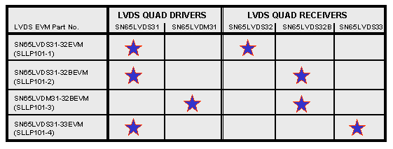
TI offers a series of low-voltage differential signaling (LVDS) evaluation modules (EVMs) designed for analysis of the electrical characteristics of LVDS drivers and receivers. Four unique EVMs are available to evaluate the different classes of LVDS devices offered by TI.
As seen (...)
SN65LVDS31-32EVM — SN65LVDS31-32EVM 評価モジュール、LVDS31 および LVDS32 用
The SN65LVDS31-32EVM evaluation moduel (EVM) includes the SV65LVDS31 quad driver and the SN65LVDS32 quad receiver. The SN65LVDS31 device is a TIA/EIA-644 standard-compliant LVDS driver. The SN65LVDS32 device is a TIA/EIA-644 standard-compliant receiver that has a passive open-circuit failsafe (...)
PSPICE-FOR-TI — TI Design / シミュレーション・ツール向け PSpice®
設計とシミュレーション向けの環境である PSpice for TI (...)
TINA-TI — SPICE ベースのアナログ・シミュレーション・プログラム
TINA-TI をインストールするには、約 500MB が必要です。インストールは簡単です。必要に応じてアンインストールも可能です。(そのようなことはないと思いますが)
TINA は DesignSoft (...)
| パッケージ | ピン数 | ダウンロード |
|---|---|---|
| SOIC (D) | 16 | オプションの表示 |
購入と品質
- RoHS
- REACH
- デバイスのマーキング
- リード端子の仕上げ / ボールの原材料
- MSL 定格 / ピーク リフロー
- MTBF/FIT 推定値
- 材質成分
- 認定試験結果
- 継続的な信頼性モニタ試験結果
- ファブの拠点
- 組み立てを実施した拠点