SLAS553B November 2008 – August 2015 TLV320ADC3101
PRODUCTION DATA.
- 1 Features
- 2 Applications
- 3 Description
- 4 Revision History
- 5 Description (continued)
- 6 Device Comparison Table
- 7 Pin Configuration and Functions
-
8 Specifications
- 8.1 Absolute Maximum Ratings
- 8.2 ESD Ratings
- 8.3 Recommended Operating Conditions
- 8.4 Thermal Information
- 8.5 Electrical Characteristics
- 8.6 Dissipation Ratings
- 8.7 I2S/LJF/RJF Timing in Master Mode
- 8.8 DSP Timing in Master Mode
- 8.9 I2S/LJF/RJF Timing in Slave Mode
- 8.10 DSP Timing in Slave Mode
- 8.11 Typical Characteristics
- 9 Parameter Measurement Information
-
10Detailed Description
- 10.1 Overview
- 10.2 Functional Block Diagram
- 10.3
Feature Description
- 10.3.1 Hardware Reset
- 10.3.2 PLL Start-up
- 10.3.3 Software Power Down
- 10.3.4 miniDSP
- 10.3.5 Audio Data Converters
- 10.3.6 Digital Audio Data Serial Interface
- 10.3.7 Audio Clock Generation
- 10.3.8 Stereo Audio ADC
- 10.3.9 Audio Analog Inputs
- 10.3.10 Input Impedance and VCM Control
- 10.3.11 MICBIAS Generation
- 10.3.12
ADC Decimation Filtering and Signal Processing
- 10.3.12.1 Processing Blocks
- 10.3.12.2
Processing Blocks - Details
- 10.3.12.2.1 First-Order IIR, AGC, Filter A
- 10.3.12.2.2 Five Biquads, First-Order IIR, AGC, Filter A
- 10.3.12.2.3 25-Tap FIR, First-Order IIR, AGC, Filter A
- 10.3.12.2.4 First-Order IIR, AGC, Filter B
- 10.3.12.2.5 Three Biquads, First-Order IIR, AGC, Filter B
- 10.3.12.2.6 20-Tap FIR, First-Order IIR, AGC, Filter B
- 10.3.12.2.7 First-Order IIR, AGC, Filter C
- 10.3.12.2.8 Five Biquads, First-Order IIR, AGC, Filter C
- 10.3.12.2.9 25-Tap FIR, First-Order IIR, AGC, Filter C
- 10.3.12.3 User-Programmable Filters
- 10.3.12.4 Decimation Filter
- 10.3.12.5 ADC Data Interface
- 10.3.12.6 Digital Microphone Function
- 10.4 Device Functional Modes
- 10.5 Programming
- 10.6
Register Maps
- 10.6.1 Control Registers
- 10.6.2 Control Registers, Page 0: Clock Multipliers and Dividers, Serial Interfaces, Flags, Interrupts and Programming of GPIOs
- 10.6.3 CONTROL REGISTERS Page 1: ADC Routing, PGA, Power-Controls, Etc.
- 10.6.4 Control Registers, Page 4: ADC Digital Filter Coefficients
- 10.6.5 Control Registers, Page 5: ADC Programmable Coefficients RAM (65:127)
- 10.6.6 Control Registers, Page 32: ADC DSP Engine Instruction RAM (0:31)
- 10.6.7 Control Registers, Pages 33-47: ADC DSP Engine Instruction RAM (32:63) Through (480:511)
- 11Application and Implementation
- 12Power Supply Recommendations
- 13Layout
- 14Device and Documentation Support
- 15Mechanical, Packaging, and Orderable Information
パッケージ・オプション
メカニカル・データ(パッケージ|ピン)
- RGE|24
サーマルパッド・メカニカル・データ
- RGE|24
発注情報
1 Features
- Stereo Audio ADC
- 92-dBA Signal-to-Noise Ratio
- Supports ADC Sample Rates From 8 kHz to 96 kHz
- Instruction-Programmable Embedded miniDSP
- Flexible Digital Filtering With RAM Programmable Coefficient, Instructions, and Built-In Processing Blocks
- Low-Latency IIR Filters for Voice
- Linear Phase FIR Filters for Audio
- Additional Programmable IIR Filters for EQ, Noise Cancellation or Reduction
- Up to 128 Programmable ADC Digital Filter Coefficients
- Six Audio Inputs With Configurable Automatic Gain Control (AGC)
- Programmable in Single-Ended or Fully Differential Configurations
- Can Be 3-Stated for Easy Interoperability With Other Audio ICs
- Low Power Consumption and Extensive Modular Power Control:
- 6-mW Mono Record, 8-kHz
- 11-mW Stereo Record, 8-kHz
- 10-mW Mono Record, 48-kHz
- 17-mW Stereo Record, 48-kHz
- Dual Programmable Microphone Bias
- Programmable PLL for Clock Generation
- I2C Control Bus
- Audio Serial Data Bus Supports I2S, Left/Right-Justified, DSP, PCM, and TDM Modes
- Digital Microphone Input Support
- Two GPIOs
- Power Supplies:
- Analog: 2.6 V to 3.6 V
- Digital: Core: 1.65 V to 1.95 V,
I/O: 1.1 V–3.6 V
- 4-mm × 4-mm 24-Pin RGE (VQFN)
2 Applications
- Wireless Handsets
- Portable Low-Power Audio Systems
- Noise-Cancellation Systems
- Front-End Voice or Audio Processor for Digital Audio
3 Description
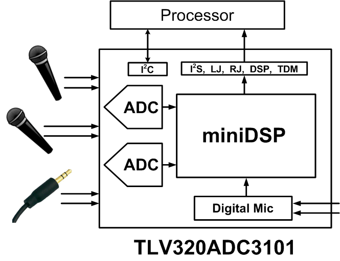
The TLV320ADC3101 device is a low-power, stereo audio analog-to-digital converter (ADC) supporting sampling rates from 8 kHz to 96 kHz with an integrated programmable-gain amplifier providing up to 40-dB analog gain or AGC. A programmable miniDSP is provided for custom audio processing. Front-end input coarse attenuation of 0 dB, –6 dB, or off, is also provided. The inputs are programmable in a combination of single-ended or fully differential configurations. Extensive register-based power control is available via an I2C interface, enabling mono or stereo recording. Low power consumption makes the TLV320ADC3101 ideal for battery-powered portable equipment.
Device Information(1)
| PART NUMBER | PACKAGE | BODY SIZE (NOM) |
|---|---|---|
| TLV320ADC3101 | VQFN (24) | 4.00 mm × 4.00 mm |
- For all available packages, see the orderable addendum at the end of the data sheet.
Functional Block Diagram
